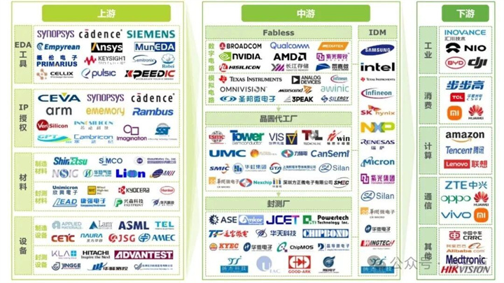
The semiconductor industry chain covers upstream software and hardware materials and equipment, midstream chip design, manufacturing, and testing, as well as downstream terminal application links.
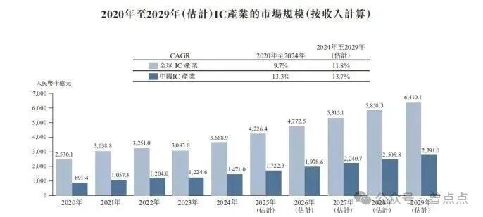
In 2024, the global semiconductor industry is expected to reach a scale of 3.67 trillion yuan, and is projected to continue growing at a compound annual growth rate of 11.8% over the next five years; The Chinese semiconductor market accounts for 40% of the global market share, with a scale of 1.47 trillion yuan. The compound annual growth rate is expected to reach 13.7% in the next five years, demonstrating broad market space and development prospects.
Upstream of the semiconductor industry chain
Upstream mainly includes key areas such as semiconductor materials, design software, and semiconductor manufacturing equipment.
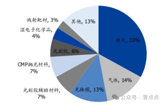
Among them, semiconductor materials can be further divided into front-end wafer manufacturing materials and back-end packaging materials. The former mainly includes silicon wafers, photoresist, etc., accounting for about 60% of the total material market size; The latter includes packaging substrates, lead frames, etc. According to data from the Semiconductor Industry Institute (SEMI), in 2022, semiconductor silicon wafers ranked first in the global semiconductor materials market share with a 33% share.
EDA software and IP core
EDA (Electronic Design Automation) is a computer software that provides support for the entire process of chip design, manufacturing, packaging, and testing, and is the cornerstone of the entire semiconductor tool chain. At present, the global EDA market presents an oligopoly monopoly pattern, with Synopsys, Cadence, and Siemens EDA accounting for a combined market share of about 70%.
In the field of semiconductor IP cores (i.e. reusable design modules), the market concentration is also high. The UK based ARM company is in an absolute leading position, with Synopsys and Cadence, which are equally strong in the EDA field, jointly occupying about 70% of the market share.
semiconductor equipment
Semiconductor equipment is mainly divided into wafer manufacturing equipment and packaging and testing equipment. According to SEMI data, in 2023, wafer manufacturing equipment sales will account for approximately 90% of the industry's total. Among them, thin film deposition, photolithography, and etching equipment are collectively referred to as the three core process equipment, with a combined market share of over 60%.
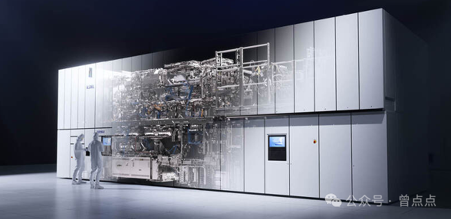
At present, China still heavily relies on imports in the fields of high-end lithography machines and measuring equipment. As a core equipment in the manufacturing process, the lithography machine is used to project circuit patterns onto silicon wafers to complete the production of microstructures. Because of this, photolithography is also the most difficult, costly, and time-consuming process in the entire chip manufacturing industry.
In this field, ASML from the Netherlands holds an absolute dominant position, not only occupying 80% of the global market share, but also being the only company in the world capable of designing and manufacturing EUV (extreme ultraviolet) lithography machines.
Midstream of the semiconductor industry chain
Chips are mainly divided into three categories: logic chips, storage chips, and analog chips.
logic chipIt is a chip that processes digital signals (0 and 1) according to preset logic, just like the "digital brain" of a device. Common CPUs and GPUs belong to this category.
This field is dominated by American companies, and the top four global manufacturers - Nvidia, Qualcomm, Broadcom, and Intel - all come from the United States. Among them, Nvidia, as an industry oligopoly, occupies nearly half of the chip design market share and is the absolute leader in the GPU field; Qualcomm dominates the mobile SoC market, with its Snapdragon series widely used in high-end models; Broadcom focuses on communication and network chips; Intel has long been at the forefront of CPU technology.
In China, well-known logic chip design companies such as Cambrian (often benchmarked against Nvidia) and Huawei HiSilicon (continuously developing under external pressure) have also emerged.
memory chipMainly used for storing data and programs, it mainly includes two types: DRAM (dynamic random access memory, often corresponding to mobile phone RAM) and NAND Flash (flash memory, often corresponding to mobile phone memory).
This field is dominated by South Korean companies, with Samsung and SK Hynix ranking in the top two globally, accounting for over half of the market share; Micron Technology from the United States ranks third. In the domestic market, Zhaoyi Innovation, as an industry leader, has successfully entered the top ten globally.
Analog chipIt is an integrated circuit that processes continuous analog signals such as sound, temperature, and voltage, playing a bridging role between the real world and digital systems. It is mainly divided into signal chain chips and power management chips.
This field is also led by American companies, with Texas Instruments (TI), Analog Devices (ADI), and Skyworks consistently ranking among the top three globally. Leading domestic enterprise Shengbang Co., Ltd. has also entered the top ten globally.
In terms of business models, chip design companies are mainly divided into two categories: Fabless (fabless) and IDM (integrated device manufacturer). The Fabless mode only focuses on the design process and outsources manufacturing, represented by companies such as NVIDIA and AMD; The IDM mode covers the entire chain from design to manufacturing, such as Samsung and Intel.
semiconductor manufacturing
When it comes to semiconductor manufacturing, many people first think of TSMC. Indeed, TSMC is the absolute leader in this field, with a global market share of over 70%.
Continuing from the previous text, chip design companies that adopt the Fabless model entrust their manufacturing processes to specialized foundries such as TSMC. Chip manufacturing belongs to high-end precision manufacturing, which requires extremely high capital and technology. Among them, the smaller the "process", the greater the technical difficulty.
The chip process is a key indicator for measuring manufacturing accuracy, usually measured in nanometers (nm), representing the minimum line width of the transistor gate. The smaller the value, the smaller the size of electronic components that can be accommodated on the chip and the higher the integration density. For example, in a 7nm process, billions of transistors can be integrated per square millimeter of chip.
At present, international leading companies such as TSMC and Samsung have achieved mass production of 3nm processes and are actively developing 2nm technology. In contrast, SMIC International, the most advanced manufacturer in Chinese Mainland, currently has a mass production process of 14nm, and still has a long way to go in catching up with technology.
Semiconductor packaging and testing
The manufactured chip needs to go through packaging and testing processes. The former provides physical protection for the chip and connects it to external circuits, while the latter is used to verify its functionality and performance. Sealing and testing is a relatively low technological threshold field in the semiconductor industry chain.
The top three companies in the global closed beta market are: Taiwan's ASE, the United States' Amkor, and Chinese Mainland's Changdian Technology. China has demonstrated strong global competitiveness in this field, with a localization rate of about 60% in the packaging and testing process.
Downstream of the semiconductor industry chain
The downstream applications of chips cover a wide range, including basic fields such as communication, computer, consumer electronics, automotive, industrial and medical, as well as deeply empowering emerging industries such as artificial intelligence, the Internet of Things, and robotics.
Chips are ubiquitous in daily life. From smartphones, televisions, computers, to cars, smartwatches, and glasses, various electronic devices rely on the collaborative work of multiple chips.
Empowering process: Semiconductor intelligent logistics
Although semiconductor intelligent logistics does not belong to the core industry chain process, it is crucial to improve the efficiency and quality of the entire industry. Semiconductor intelligent logistics can achieve automated, intelligent, and unmanned material handling, storage, and information management within the factory area. Ensure the safe transmission of high-value and high-precision wafers and chips in ultra clean environments. Improve production efficiency, reduce human error and pollution. Through data tracing, achieve lean management throughout the entire process. It is one of the key supports to help semiconductor companies build lighthouse factories and achieve Industry 4.0.
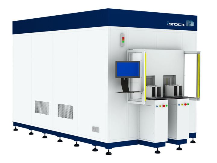
I-stock always adheres to customer needs as the core, driven by intelligent equipment and precision technology, industrial software connects data flow, data+AI algorithm empowers smart warehousing in the electronics and semiconductor industries, focuses on product quality, and serves with dedication. I-stock helps enterprises solve practical problems encountered in the scientific, standardized, digital, automated, and intelligent upgrading of smart warehousing, and provides customized services for smart warehousing equipment.
In the future, i-stock will continue to leverage its advantages in technical talent and resources to contribute to the transformation and upgrading of China's manufacturing industry. In this process, i-stock will help more companies enter the lighthouse factory and work together to promote China's manufacturing industry to the top of the global value chain.