

Traditional packaging processes first "cut" silicon wafers into individual chips, then mount these chips onto a printed circuit board (PCB) and establish electrical connections; On the other hand, wafer level packaging involves electrical connections and plastic packaging at the wafer level, followed by laser cutting and separation of the chips.
In terms of chip structure, the biggest difference between Wafer Level Chip Scale Packaging (WLCSP) and Flip Chip is that there is no substrate between the die of WLCSP and the PCB. On the contrary, it replaces the substrate with Redistribution Layers (RDL), achieving a smaller packaging volume and improving thermal conductivity efficiency.
Classification of wafer level packaging
There are two main types of wafer level packaging: Fan In and Fan Out.
Fan in wafer level packaging:
Mainly used for low-end mobile phones with lower technical requirements. In this packaging method, the routing direction of the rewiring layer (RDL) is oriented towards the center of the chip.
Fan out wafer level packaging:
Launched in 2007. In this packaging structure, the size of the rewiring layer (RDL) and solder balls exceeds that of the chip itself, so the chip can have more input/output interfaces (I/O) while maintaining thinness.
Fan out packaging is further divided into three categories: Core, High Density, and Ultrahigh Density. The specific differences are as follows:
Core type:
Mainly used in automotive and network application scenarios with low technical requirements (such as RF chips, information and entertainment chips). In the fan out packaging market with a scale of nearly 1.5 billion US dollars, the proportion of core packaging is less than 20%.
High density and ultra-high density types:
Mainly applied in the field of mobile devices, it is expected to expand to some network applications and high-performance computing (HPC) application scenarios in the future.
Currently, the world's largest wafer level chip size package (WLCSP) manufacturer is Taiwan Semiconductor Manufacturing Corporation (TSMC).
The development of stacked wafer level packaging
Over the past decade, stacked wafer level packaging technology has gradually matured. This technology can integrate multiple integrated circuits (ICs) within the same package, suitable for both "hetero bonding" (i.e. integrating logic chips with storage chips) and storage chip stacking.
1. 2.5-D Stacking
2.5D stacking technology arranges two or more chips side by side and connects them through an intermediate layer (Interposer). According to the different types of intermediaries used, 2.5D stacking can be divided into the following categories:
Silicon Interposers:
It is currently the only type of intermediate layer that requires the use of Through Silicon Via (TSV). Silicon via is a vertical electrical connection structure that can penetrate through silicon chips or wafers. The technology used in the silicon intermediate layer is relatively mature and has been applied in the market for more than ten years, but the cost of silicon materials is high and requires advanced front-end processes and manufacturing capabilities to support. Currently, TSMC's CoWoS-S (Chip on Wafer on Substrate) technology dominates the market in this field.
Silicon Bridges:
It belongs to a relatively new technology. Compared with traditional silicon interlayers, silicon bridges use less silicon material, resulting in thinner thickness, which helps reduce power consumption and improve design flexibility. Its core advantage lies in supporting more advanced system level integration, making it commonly used in high-performance computing (HPC) scenarios such as artificial intelligence (AI). Representative technologies include Intel's Embedded Multi Chip Interconnect Bridge (EMIB) and TSMC's CoWoS-L technology.
Rewiring layer (RDL):
It can also be used as an intermediary. The biggest advantage of this technology is that the photolithography process for producing rewiring layers can achieve fine circuit patterns, thereby improving speed gain and heat dissipation efficiency. At present, TSMC's CoWoS-R (chip on wafer overlay substrate based on rewiring layer) technology is ready to enter the mass production stage.
Glass Interposers:
As the next generation of intermediary materials is emerging. Glass materials have the advantages of low cost and low power loss under high frequency bandwidth, but it may be difficult to achieve market-oriented applications in the short term.
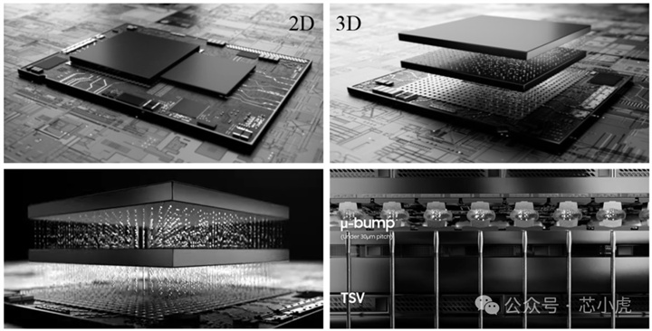
2. 3D Stacking
3D stacking technology stacks multiple chips face down (whether or not an intermediate layer is used), mainly divided into two types:
Silicon via (TSV) technology with µ - bumps:
It is currently the most common type of 3D stacking.
Bumpless Hybrid Bonding Technology:
It belongs to a relatively new alternative solution. This technology achieves chip to chip interconnection through dielectric bonding and embedded metals, and currently only manufacturers in the storage field are exploring it.