

Cutting process flow
After the wafer goes through the previous process, the chip preparation is completed, and it needs to be cut to separate the chips on the wafer, and finally packaged. The wafer cutting processes selected for wafers of different thicknesses are also different:
Wafers with a thickness of over 100um are generally cut using blades;
Wafers with a thickness of less than 100um are generally cut using laser cutting, which can reduce the problems of peeling and cracking. However, when the thickness is above 100um, production efficiency will be greatly reduced;
For wafers with a thickness of less than 30um, plasma cutting is used. Plasma cutting is fast and will not cause damage to the wafer surface, thereby improving yield. However, the process is more complex;
Blade dicing or blade sawing
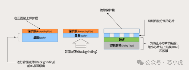
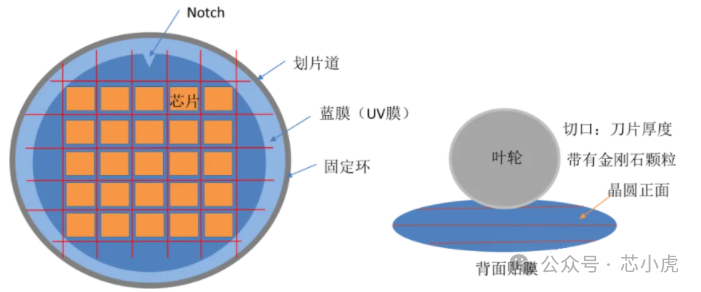
In order to protect the wafer from external damage during the cutting process, a film of adhesive is applied to the wafer in advance to ensure safer "cutting". During the 'Back Grinding' process, the adhesive film will be attached to the front of the wafer. On the contrary, in "blade" cutting, the adhesive film needs to be attached to the back of the wafer. During the process of eutectic bonding (die bonding, which fixes separated chips on a PCB or fixture), the adhesive film on the back of the chip will automatically peel off. Due to the high friction during cutting, DI water (deionized water) needs to be sprayed continuously from all directions. Moreover, the impeller should be attached with diamond particles for better slicing. At this point, the incision (blade thickness: width of the groove) must be uniform and not exceed the width of the cutting groove.
For a long time, sawing has been the most widely used traditional cutting method, and its biggest advantage is that it can cut a large number of wafers in a short period of time. However, if the feeding speed of the slice is significantly increased, the possibility of edge peeling of the small chip will increase. Therefore, the number of rotations of the impeller should be controlled at around 30000 times per minute.
Wafer cutting machine
When wafer cutting, narrow street widths are often encountered, requiring the ability to place each cut within a few micrometers of the center of the street. This requires the use of equipment with high indexing axis accuracy, high optical amplification, and advanced alignment calculations. When cutting wafers with narrow tracks, the thinnest blade possible should be selected. However, very thin blades (20 µ m) are very fragile and more prone to premature rupture and wear. As a result, the lifespan and process stability of the blade are relatively poor compared to thicker blades. For blade thickness of 50-76 µ m track, it should be 20-30 µ m.
Knife marks, automatically calibrate the position of the reference line to prevent excessive edge breakage and loss of yield caused by slicing. Accurate height measurement and real-time detection of cutting blades during synchronous cutting operations. The cleaning area is equipped with a water vapor two fluid cleaning device, which can efficiently clean the processed materials. The Disco DAD36501 semi-automatic slicer is capable of operating 8-inch wafers, including automatic optical compensation, focusing, and self recognition of feature points. It is equipped with two types of lenses, high and low magnification, and can be used for measuring the width of cutting tracks, adjusting reference lines, and more. It can automatically detect cutting marks and calibrate the position of the reference line to prevent excessive edge breakage and loss of yield caused by slicing. Accurate height measurement and real-time detection of cutting blades during synchronous cutting operations
Key points of slicing process
1、Chipping
Top side chipping (TSC) occurs on the top surface of the wafer, becoming a pass rate issue. When slicing approaches the active area of the chip, it mainly relies on blade grit size, coolant flow rate, and feed rate. Back side chipping (BSC) occurs on the bottom surface of the wafer when large, irregular small cracks spread and merge from the cut bottom surface (Figure 1b). When these small cracks are long enough to cause unacceptable large particles to be removed from the incision, BSC becomes a pass rate issue. If the size of the back fragments is below 10 µ m, ignore it. On the other hand, when the size exceeds 25 µ m, it can be considered as potential damage. However, an average size of 50 µ m is acceptable, depending on the thickness of the wafer.
Collaboration between the slicing system and the blades is necessary to meet new slicing challenges. This is particularly true for high-end applications. Blades play a major role in process optimization. In addition to size, three key parameters determine blade characteristics: diamond (abrasive) size, diamond content, and type of binder. A composite is a matrix composed of various metals and/or diamond abrasives distributed within them. Other factors, such as feed rate and spindle speed, may also affect blade selection. The relative importance of the three key blade elements (diamond size, concentration, and bond hardness) depends on the blade abrasive size and process parameters. Understanding these relationships is necessary in order to select the most suitable blade for a specific application.
2、Blade Load Monitering
During slicing or any other grinding process, the new generation slicing system can automatically monitor the load or torque applied to the blade without exceeding acceptable cutting quality parameters. For each set of process parameters, there is a limit torque value for slice quality degradation and BSC occurrence. The relationship between cutting quality and the interaction force between the blade substrate, as well as the measurement of its variables, enables the determination of process deviations and damage formation. The process parameters can be adjusted in real-time to ensure that the torque limit is not exceeded and the maximum feed rate is achieved. The key part of the slicing process is the dressing of the cutting blade. In non monitored slicing systems, the trimming process is established through a set of repeated experiments. In the system where blade load is monitored, the endpoint of trimming is discovered through measured force data, which establishes the optimal trimming procedure. This method has two advantages: it does not require a time limit to ensure optimal blade performance, and there is no loss of pass rate due to poor quality caused by slicing with partially trimmed blades.
3、Coolant Flow Stabilization
A system that operates with stable torque requires stable feed rate, spindle speed, and coolant flow rate. The coolant exerts resistance on the blade, causing torque. The latest generation slicing system maintains stable flow rate and resistance by controlling the coolant flow rate, thereby ensuring the stability of the coolant torque effect. When the slicer has a stable coolant flow rate and all other parameters are controlled, maintain a stable torque. If recorded, any deviation from stable torque is due to uncontrolled factors. These include changes in coolant flow due to nozzle blockage, changes in nozzle adjustment, blade to blade changes, blade conditions, and operator errors. The slicing process is becoming increasingly demanding. The narrower the cutting path, the more likely it is to fill the test pad, and the blade may need to cut various coating layers made of different materials. To achieve the maximum slicing process qualification rate and productivity under these conditions, careful blade selection and advanced process control capabilities are required.
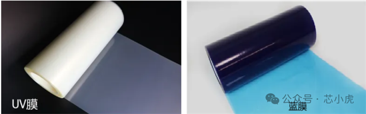
The difference between wafer UV film and blue film
Before the wafer is sliced, a layer of film is attached to the back of the wafer. The function of this film is to stick the chip to the film, which can maintain the integrity of the grains during the cutting process and reduce problems such as breakage, displacement, and falling during the cutting process. In actual production, UV film or blue film is generally used to fix wafers and chips.UV film: mainly used for wafer thinning process;
Blue film: mainly used for wafer slicing process;
1. Characteristics of UV film and blue film
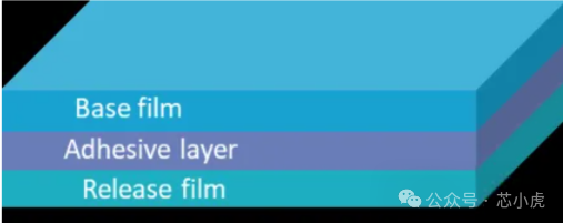
UV film and blue film both have adhesiveness, and the degree of adhesiveness is generally expressed by the degree of adhesive peeling, usually measured in units of N/20 mm or N/25 mm. The meaning of 1 N/20 mm is that the width of the test strip is 20mm, and the force required to peel it off from the test board at a 180 ° peeling angle is 1N. UV film is a special formula coating applied to the surface of PET film substrate to achieve the effect of blocking ultraviolet light and short wavelength visible light. Figure 2 shows the structure diagram of a universal UV film.
Generally, UV film consists of three layers, with polyethylene chloride as the base material, a viscous layer in the middle, and a release film adjacent to the viscous layer. Some UV film models do not have this coating.
UV film is usually called ultraviolet irradiation tape, which is relatively expensive and has a shorter shelf life when not in use. It is divided into three types: high viscosity, medium viscosity, and low viscosity. The high viscosity UV film has a viscosity of 5000mN/20mm~12000mN/20mm without UV irradiation, and after UV irradiation, the peel viscosity is below 1000mN/20mm; The peel viscosity of low viscosity UV films without UV irradiation is around 1000mN/20mm, but after UV irradiation, the peel viscosity decreases to around 100mN/20mm. After UV irradiation, the low viscosity UV film will not have any residual adhesive on the surface of the wafer, and the grains are easy to remove. UV film has appropriate expandability, and during the thinning and slicing process, water will not penetrate between the grains and the tape.
Blue film is usually called electronic grade tape, with a lower price. It is a type of blue film with constant viscosity, and its adhesive peel off degree is generally between 100~3000mN/20mm. It may produce residual adhesive due to temperature. In contrast, UV film is more stable than blue film.
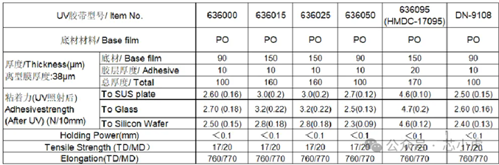
Sliontec UV tape
features:
a、 Complete variety, with various thicknesses of adhesive layer (5-25um);
b、 Reduce back breakage and prevent flying materials, as well as chip splashing;
c、 Implement Easy Pick up (easy to peel off);
d、 It also has high-quality adhesion for difficult to bond workpieces such as EMC (Epoxy Molding Compound semiconductor epoxy synthetic polymer packaging material);
e、 Anti static type (option).
List of parameter specifications:
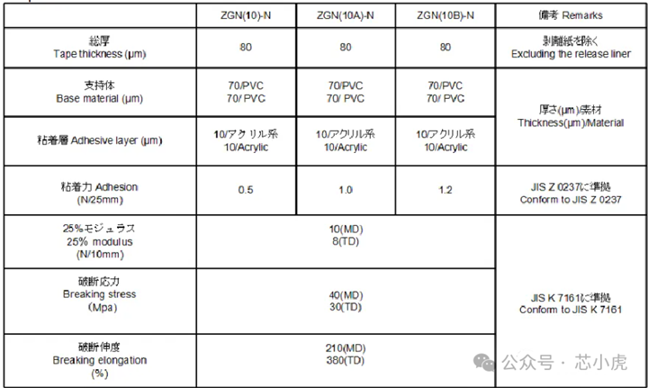
Maruishi Blue Film
features:
a、 Has good adhesive stability
b、 Has good picking and peeling performance.
c. The PVC substrate is thin, and the tape has good expandability.
d、 Meets Rohs 2.0 requirements.
e、 Suggested chip size is between 0.8 mmsq and 5 mmsq.
List of parameter specifications:
2. Application analysis of UV film and blue film in production
Generally speaking, UV film is used for thinning and slicing of small chips, while blue film is used for thinning and slicing of large chips. This is because the viscosity of the UV film can be controlled by the duration and intensity of UV irradiation to prevent chips from being missed or broken during the grabbing process. If the chip is directly placed on the reverse packaging label production line after thinning and scratching, it is best to use UV film because the chips in the reverse packaging production line are generally small, and the top pin of the equipment lifts the chip at the bottom of the blue film. If a blue film with a high degree of adhesive peeling is used, it may cause the ejector pin to break the chip during the process of lifting it up.
Due to the temperature effect, the viscosity of the blue film will change, and its viscosity is relatively high. Therefore, for chips or wafers with larger areas that are thinned and cut, the post packaging process is usually carried out directly instead of the reverse packaging process for Inlay. Therefore, blue film can be considered for use.
Compared with blue film, UV film has great advantages due to its variability in adhesive peeling degree. Its main function is to fix the wafer during the thinning process; During the wafer cutting process, it is used to protect the chip from falling off or chipping; Used for flipping and transporting wafers to prevent the already scratched chips from falling off. Standardize the use of various parameters of UV film and blue film, and select the appropriate UV film or blue film according to the processing technology required for the chip, which can save costs and also contribute to the development of chip industrialization.

Image and text reprint from "Xin Xiao Hu"