Why are chips square and wafers round?

In the semiconductor manufacturing process, all manufacturing steps of the chip before cutting and packaging are carried out on the wafer. However, the finished chips we see are usually square, and manufacturing chips on circular wafers can result in some areas being underutilized. So, why not use square wafers to improve utilization?
In fact, the answer to this question is simple: because wafers (originally in the form of silicon wafers) are cut from cylindrical silicon rods, their cross-section can only be circular. So, why are silicon rods cylindrical?
From the upstream industry of semiconductor manufacturing, namely the manufacturing process of silicon wafers and wafers. Firstly, it is necessary to understand the preparation of monocrystalline silicon. Monocrystalline silicon is the basic material for manufacturing chips, which can be extracted from quartz sand. The main component of quartz sand is silicon dioxide (SiO ₂), which can be purified and prepared to obtain high-purity polycrystalline silicon.
In 1916, Polish chemist Jan Czochralski accidentally immersed a pen in a melted tin crucible instead of an ink bottle. When he quickly pulled out the pen, he found a solidified metal wire hanging from the tip of the pen. Through experiments, he confirmed that this metal wire is composed of single crystals of metal, with a diameter reaching the millimeter level. Afterwards, scientists improved this method and eventually developed the technology for manufacturing single crystal silicon, which is called Czochralski method or Czochralski method.
Monocrystalline silicon corresponds to polycrystalline silicon. Polycrystalline silicon is composed of many small grains, and the arrangement between these grains is irregular. Single crystal silicon itself is a complete large grain, in which atoms or ions are arranged in an ordered pattern. Due to the fact that polycrystalline silicon does not have a repetitive single crystal structure like monocrystalline silicon, it cannot provide stable electrical and mechanical properties. Therefore, the silicon wafers used for chip manufacturing can only be monocrystalline silicon.
In summary, the reason why silicon rods are cylindrical is because the direct drawing method is used in the preparation process of single crystal silicon. This method determines the shape of the silicon rod. Circular wafers are more in line with this production process, so although some areas are not fully utilized, circular wafers are still chosen as the basis for manufacturing chips.
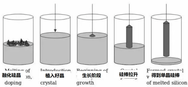
The process of Czochralski: Firstly, high-purity silicon is heated to a molten state in a crucible. Next, place a seed crystal at the end of a precisely oriented rod and immerse its end into the molten silicon. Subsequently, the rod is slowly lifted and rotated simultaneously. By strictly controlling the pulling speed, rotation speed, and temperature, a larger cylindrical monocrystalline silicon rod can be formed at the end of the rod. Afterwards, the silicon rod undergoes processes such as grinding, polishing, and cutting to obtain circular silicon wafers that can be used for chip manufacturing.
Therefore, the circular shape of the wafer is mainly determined by the shape of the silicon rod. However, strictly speaking, wafers are not completely circular. Normally, after the silicon wafer is processed into a wafer, a notch is ground at the edge. For silicon wafers with a diameter less than 200 millimeters, a flat corner is usually cut; For silicon wafers with a diameter greater than 200 millimeters, a small incision will be made. The purpose of doing this is to indicate the growth direction of the silicon crystal, and also to facilitate the positioning operation in subsequent photolithography and etching steps.
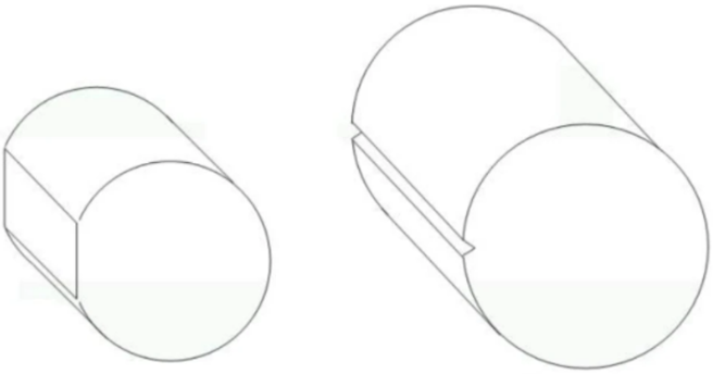
In fact, the silicon rod can be cut into rectangular shapes before slicing, so that the "crystal square" can be directly obtained during subsequent slicing. However, silicon rods used for chip production usually do not do this for the following reasons:
Firstly, a circular shape is more advantageous for photoresist coating. Before photolithography, a uniform layer of photoresist needs to be applied to the surface of the wafer, and the uniformity of the coating directly affects the yield of the chip. The commonly used coating method currently is to coat the center of the silicon wafer with photoresist, and then evenly distribute the photoresist on the entire wafer through rotation. Due to the viscosity, surface tension, and air resistance of liquids, the four corners of square wafers are prone to photoresist accumulation during spin coating, which can affect the overall effect of lithography, reduce yield, and cause more waste.
Secondly, circular wafers have higher structural strength. Before becoming a wafer, silicon wafers need to go through complex processes such as photolithography, etching, and chemical polishing. During these processes, the wafer will accumulate more stress on the outer ring, and the sharp corners of square wafers will cause stress concentration at the edges, which can easily lead to damage during production and affect the overall yield rate.
As for why some wafers do not have chips on the outer ring, while others have incomplete chips even on the outer ring, it is because the design and layout of the wafers are different. In some designs, the outer ring area is left blank to prevent damage caused by edge stress and improve overall yield. In other designs, although there may be incomplete chips in the outer ring area, these areas are usually marked for removal in subsequent processes to ensure that only good products enter the next step.
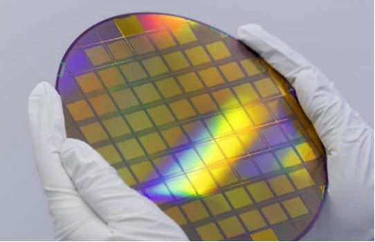
This is actually related to the size of the photomask used in the photolithography process. The basic principle of photolithography is to expose a silicon wafer coated with photoresist to a specific light source (such as EUV extreme ultraviolet light), and form the desired circuit pattern on the wafer surface through a photomask. The photomask itself is square and composed of many grids, each called a Shot, which is the smallest unit of exposure. Each Shot contains one or more Dies and peripheral testing circuits. Since Shot is square, Die is also square. The size of the photomask usually covers all areas of the wafer, so incomplete shots may appear at the edges of the wafer.
In addition, edge effects are also an important factor. If peripheral circuits are not made, the difference in material density between the edge and center of the wafer will have an impact on the overall yield rate. To cope with this situation, even at the edge of the wafer, it is necessary to make some incomplete shots to ensure that the material density at the edge and center is consistent.
Industry experts have provided a detailed explanation of this phenomenon: "During the chip manufacturing process, the wafer will continuously thicken, especially in the later stages of metal and through-hole production processes, where multiple CMP (chemical mechanical polishing) processes will be used. If there is no pattern on the edge of the wafer, the edge polishing rate will be too slow, resulting in a height difference between the edge and the center.This height difference will affect adjacent intact chips during the subsequent grinding process. Therefore, even as a dummy pattern, incomplete shots at the edge of the wafer need to be exposed normally to ensure overall consistency.
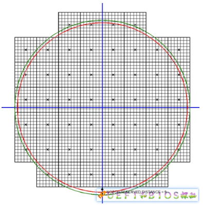
However, chips on the outer edge of the wafer are usually not used. As mentioned earlier, due to the production process, there is inevitably a certain amount of stress at the edge of the wafer. Chips produced in this area also retain stress internally, making them more susceptible to damage during subsequent cutting, packaging, and transportation processes. Therefore, current manufacturers usually choose to lay circuits on the entire wafer when using large-area wafers to produce chips, in order to improve yield. This is also why some wafers have chips on the outer ring, while others do not.
Overall, using circular wafers for chip manufacturing has a high yield rate. However, why can't chips be designed in a circular shape?
In fact, the manufacturing of circular chips is more complex. After a series of processes such as coating, photolithography, etching, and ion implantation are completed on silicon wafers, chips are manufactured. But at this point, the chip is still connected to the wafer and needs to be cut to become an independent entity.
Imagine that a square chip can be completely separated with just a few cuts. Circular chips require more time for cutting, which may be several times longer than square chips. From a packaging perspective, square chips are also more convenient for wire handling, even when using Flip chip type packaging, square chips are easier to machine operate for aligning I/O interfaces with solder pads.
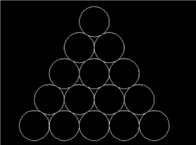
The most crucial point is that circular chips cannot solve the problem of wasted silicon wafer area. Cut out many square areas on a wafer, with no gaps between these areas, and only a small amount of unused space at the edge of the wafer. However, if many circular areas are cut from a plane, it will inevitably create some wasted space in the middle and also lead to waste at the edge of the wafer.
Actually, saving wafer area has always been an important issue. The more chips that can be produced on a wafer, the higher the production efficiency and the lower the cost of a single chip. The best way to solve production efficiency at present is to increase the wafer area, which is the calculus we are familiar with.
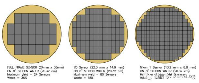
From the picture, it can be simply seen that when the chip area is fixed, using larger wafers can effectively improve wafer utilization. According to the calculation formula commonly used by Fab factories internationally:

Producing 100mm ² chips on a 12 inch wafer can produce approximately 660 chips, while using an 8-inch wafer only yields 180 chips, reducing the wafer area by 50% but reducing the number of chips by 72%. Therefore, currently 12 inch wafers have become the main battlefield for larger IDM and foundry manufacturers worldwide. At present, only a small number of enterprises in our country have the manufacturing technology of 12 inch semiconductor silicon wafers, and domestic enterprises are accelerating to catch up with the world's leading companies.
From the perspective of wafer utilization, current chip designs no longer use circular chips, but generally use square chips. However, the so-called 'wafer' is still circular, which is common in the industry.
In addition to being used for manufacturing chips, silicon wafers also play a crucial role in the field of photovoltaics. Photovoltaic power generation utilizes the photovoltaic effect of silicon wafers to directly convert solar radiation into electrical energy. Both polycrystalline and monocrystalline silicon can generate photovoltaic effects. However, single crystal silicon has a more complete crystal structure, more uniform optical and electrical properties, higher mechanical strength, and higher photoelectric conversion efficiency. Therefore, the conversion efficiency of single crystal cells is usually 2 to 3 percentage points higher than that of polycrystalline cells.
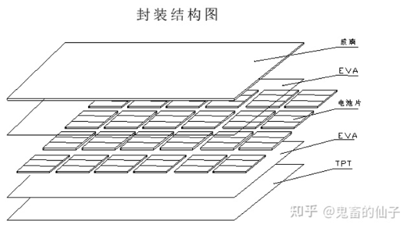
The early stage of the preparation process of photovoltaic monocrystalline silicon is the same as that of chip monocrystalline silicon, which involves heating high-purity silicon to a molten state and then pulling out a monocrystalline silicon rod from it. Before slicing, the photovoltaic silicon will first cut the silicon rod into rectangular shapes, so that the cross-section of the silicon wafer becomes square. The reason for using a square shape is also very simple. If the photovoltaic cell is circular, multiple cells arranged in the middle of the solar panel will create gaps, reducing the overall conversion rate.
Compared with chips, the requirement for silicon purity in the manufacturing of photovoltaic panels is slightly lower, with a purity standard of only 99.9999%, which cannot meet the 99.99999999% required for chip production.
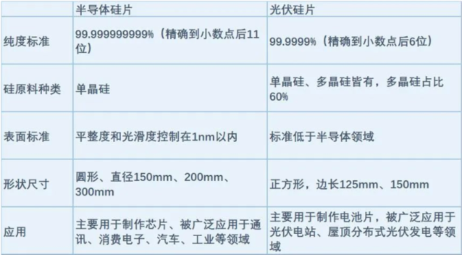
Why is the chip square? Circular chips are difficult to cut, and the subsequent packaging stage is also inconvenient to control. Most importantly, circular chips cannot solve the problem of wasted wafer area. Why are wafers round? In the process of producing chips, circular wafers are more convenient to produce and have higher yield due to mechanical factors, and the silicon rods are naturally cylindrical, so the wafers are naturally circular. However, in the field of photovoltaics, square silicon wafers do not waste space during cell packaging, so square silicon wafers are used for photovoltaics.

Partial graphic and textual references from RFID World Network


