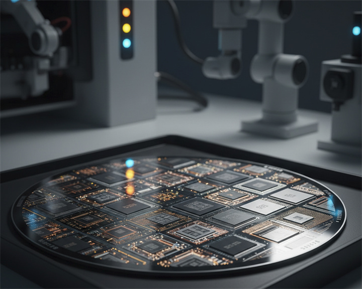
1. Causes of Wafer Warping
Wafer warping is not caused by a single factor but results from macroscopic deformation triggered by the interaction between material intrinsic properties and complex processes under the coupled effects of thermal, mechanical, and chemical multiphysics. Its core lies in stress generation exceeding the structural stiffness limit.
1. The mismatch of intrinsic properties of materials is the physical basis
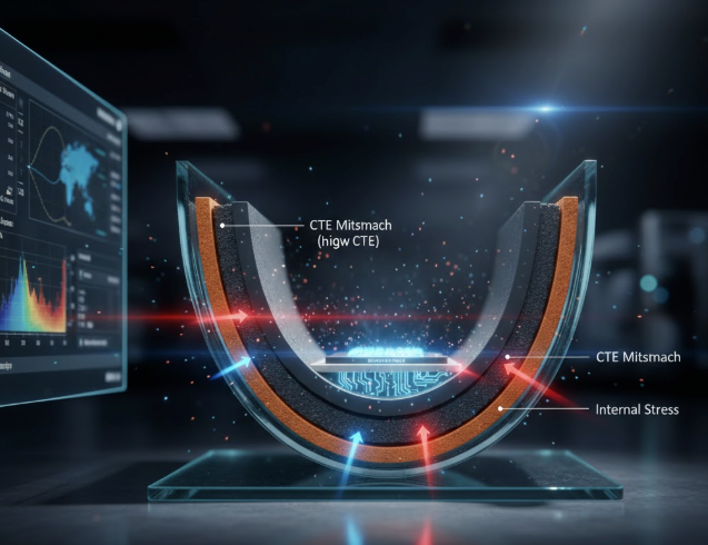
• Mismatch of thermal expansion coefficient:This is the fundamental cause of thermal stress. Silicon (~2.6 ppm/° C), encapsulation polymers (such as EMC, 7-20 ppm/° C), copper (~17 ppm/° C), and other materials experience asynchronous expansion and contraction during temperature cycling (such as reflow peak above 260 ° C), resulting in significant interfacial shear stress and overall bending moment. In 2.5D/3D packaging, the CTE gap between the silicon interlayer and the organic substrate is the main source of warpage.
• Modulus (stiffness) mismatch:High modulus materials (such as silicon and metals) and low modulus materials (such as polymers and adhesives) deform incongruously under stress, resulting in stress concentration at the interface. For example, a rigid chip is surrounded by a soft bottom filling material, and the deformation of the filling material will be constrained by the chip when the temperature changes, and vice versa.
• Material properties evolve with process:The volume shrinkage, curing degree changes, and glass transition temperature of polymer materials (such as PI and EMC) during the curing process can dynamically alter their modulus and CTE, making the stress state extremely complex.
2. Advanced manufacturing processes involve direct introduction of stress and amplification
• Inherent stress of thin film deposition:Chemical vapor deposition thin films (such as SiN, SiO ₂) have intrinsic stresses, which originate from the non-equilibrium stacking of atoms/molecules during the film growth process. They can be divided into tensile stress and compressive stress, with values ranging from several hundred megapascals to gigapascals. The layer by layer accumulation of these stresses is an important reason for the warpage of wafers before packaging.
• Visualization and heterogeneous integration disrupt structural integrity:The processes of deep silicon etching to form TSV and laser drilling create stress concentration points in the wafer. The local stiffness enhancement effect brought by metal routing (RDL) contrasts sharply with the dielectric layer region, resulting in a "landscape style" stress distribution. The mixed bonding or micro bump connections in 3D stacking introduce new and unpredictable interface stresses.
• Mechanical challenges of wafer thinning and temporary bonding:Grinding the wafer to below 100 µ m (even 25 µ m) causes a sharp decrease in its bending stiffness in a thickness cubic relationship, making it extremely sensitive to stress. The viscoelastic relaxation of temporary bonding adhesive at high temperatures, CTE mismatch between the substrate and wafer, and energy impact during debonding (whether mechanical peeling, laser ablation, or thermal slip) are all high-risk warpage inducing processes.
3. The design topology determines the stress distribution pattern
• Geometric asymmetry:Almost all advanced packaging structures are asymmetric stacks (such as multiple layers of RDL and bumps on the front, and only a thin passivation layer on the back). This causes the neutral plane of the structure to deviate significantly from its geometric center plane, resulting in even small stress differences being amplified into significant bending deformations during temperature changes.
• Uneven pattern density:The metal density in the core area of the chip (>80%) differs significantly from that in the peripheral and cutting areas (<10%), resulting in different effective CTE and equivalent modulus in local areas of the wafer. This "mosaic" material distribution can cause complex, non spherical high-order warping patterns, posing great challenges to global leveling in photolithography.
2、 The impact of warping
The impact of warping is a full process and chain reaction:
• Process feasibility risk:In the photolithography process, excessive distortion can exceed the depth of focus tolerance, resulting in pattern distortion or inability to expose simultaneously. During the bonding and mounting process, warping leads to poor coplanarity, resulting in uneven pressure on micro bump connections, voids, or bridging, which directly affects the reliability of electrical connections.
• Mechanical integrity risk:Warped wafers are prone to breakage during transportation, grinding, and cutting processes. The larger residual stress is also a potential source of cracking and delamination in the subsequent module assembly or terminal use of the chip.
• Long term reliability risk:Warping is an external manifestation of the presence of significant residual stresses inside the package. These stresses will become the driving force for fatigue crack initiation and propagation under the temperature and power cycling service conditions of the product, accelerating failures such as solder joint failure and dielectric layer rupture.
3、 Systematic improvement measures
The warpage management of modern advanced packaging has shifted from post process repair to active stress engineering that runs through the entire chain of design, materials, process, and simulation.
1. Innovation and selection at the material level
• Develop advanced packaging specialized materials:Develop bottom fillers, molding compounds, and dielectric materials with low shrinkage, low modulus, and adjustable CTE. For example, introducing nano silica or elastomer microspheres into epoxy resin can reduce CTE while maintaining a certain level of toughness to absorb stress.
• Implement stress matching design:Consciously using CTE gradient transition materials in stacked designs, such as inserting an intermediate layer of medium CTE between the chip and the high CTE substrate to mitigate stress transients.
• Precise control of thin film stress:By changing the deposition process parameters (such as temperature, pressure, power, gas ratio) or using multi-layer stress compensation structures (such as alternating compressive and tensile stress films), the total stress of the thin film stack can be controlled to approach zero.
2. Optimization at the structural and design level
• Forced Symmetrical Design:After completing the front process, deposit an active stress balancing layer on the backside of the wafer. The thickness and stress of this layer of material (such as SiN or metal layer under specific stress) are precisely calculated to generate a reverse torque that "flattens" the warpage. This is one of the most effective design methods for dealing with high-order warping.
• Layout density homogenization:Systematically insert virtual metal patterns into the cutting lines and low-density areas to achieve the most uniform distribution of metal/dielectric on the entire wafer surface, thereby eliminating local stresses caused by differences in pattern density.
• Strategic selection of carriers and intermediaries:For high-precision 2.5D packaging, it is preferred to use silicon or glass interlayers that are almost compatible with the chip CTE, rather than traditional organic substrates, to significantly reduce thermal mismatch from the carrier end.
3. Fine control and innovation at the process level
The combination thinning process of "grinding+chemical mechanical polishing+wet/dry etching" is adopted to remove the damage layer caused by mechanical grinding and obtain a low stress, smooth back surface.
• Optimize temporary bonding system:Develop a combination of "rigid carrier board+low modulus, high-temperature stable release adhesive" to provide rigid support during the manufacturing process, while also gently and uniformly releasing stress during debonding.
• Low temperature and low-temperature process:Vigorously develop low-temperature bonding (such as surface activated bonding) and low-temperature deposition processes to fundamentally reduce the source of thermal stress.
• Introduce stress relaxation step:After key high stress processes such as thin film deposition and high-temperature curing, strategically insert annealing technology to allow sufficient kinetic energy for the atoms/molecules inside the material to rearrange and release some internal stress.
• Advanced thinning and support technology:
The combination thinning process of "grinding+chemical mechanical polishing+wet/dry etching" is adopted to remove the damage layer caused by mechanical grinding and obtain a low stress, smooth back surface.
Optimize temporary bonding system: Develop a combination of "rigid carrier board+low modulus, high-temperature stable release adhesive" to provide rigid support during the process, while also gently and uniformly releasing stress during debonding.
4. Digital empowerment at the level of prediction and monitoring
• Predictive Design Based on Simulation:In the early stage of product development, use finite element analysis and other computational tools to establish a detailed model that includes all material nonlinearity (temperature related CTE, modulus), curing shrinkage, viscoelasticity, and other behaviors. Through virtual "trial and error", predict the warping trend in advance, optimize the stacking sequence, material selection, and structural dimensions, and achieve "correct for the first time".
• Full process online monitoring and feedback control:Deploy automated warpage measurement equipment at key nodes on the production line (such as after thinning and bonding) and establish a warpage data graph. By analyzing the correlation with process parameters, dynamic process window adjustment and feedforward/feedback control are achieved to ensure that warpage is always within a controlled range.
4、 Summary and Frontier Outlook
Wafer warpage is an inevitable accompanying challenge for the development of advanced packaging towards higher integration, thinning, and heterogeneous integration. The solution has evolved from a single process adjustment to a comprehensive discipline involving materials science, solid mechanics, process engineering, and computational science.
Frontier research directions include:
• Smart Materials:Develop adaptive materials that can perceive and actively compensate for stress.
• Atomic scale simulation:Understand the generation and evolution mechanism of interface stress from a more microscopic perspective.
• AI/ML driven process optimization:Using machine learning algorithms to find the optimal solution among massive process parameters and warping data, achieving adaptive process control.
Essentially, the ability to effectively control warping has become one of the core competencies for measuring whether a company or a technology platform can achieve mass production of next-generation advanced packaging (such as 3D SoIC, chip heterogeneous integration).