In today's semiconductor industry, which continues to pursue higher performance, lower power consumption, and smaller size, advanced packaging technology has become an important engine driving chip development. CoWoP, CoWoS, and CoPoS, as the three mainstream 2.5D/3D packaging technologies, are often mentioned by industry insiders, but their differences and application scenarios have left many people confused. This article will provide you with a detailed analysis of the similarities and differences among these three technologies.
Current Overlord: The Brilliance and Challenges of CoWoS Technology
CoWoS (Chip on Wafer on Substrate)
CoWoS, as an advanced packaging technology led by TSMC, has become an indispensable infrastructure in the AI era. This technology achieves high-density integration of processors, accelerators, and high bandwidth storage (HBM) by mounting bare chips on silicon wafers and combining them with silicon intermediate layers, and then encapsulating them on organic substrates.In terms of technical principle, CoWoS adopts a four layer structure: silicon chip+intermediate layer+organic packaging substrate+PCB motherboard. The micro bump inversion technology connects the chip to the silicon intermediate layer, and then connects it to the motherboard through the packaging substrate. This design significantly shortens the distance between chips, improves bandwidth and energy efficiency, allowing AI accelerators such as NVIDIA A100/H100 to fully utilize their performance.
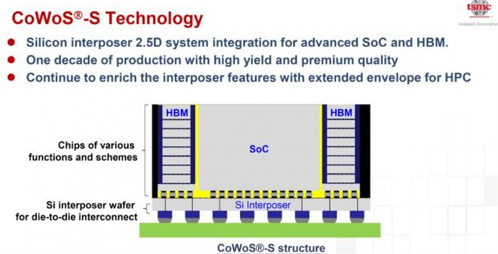
CoWoS has evolved over multiple generations, including:
CoWoS-S: Standard Silicon Interlayer Version
CoWoS-R: Replacing Part of Silicon Intermediary with Re routing Layer (RDL)
CoWoS-L: Combining local silicon interconnects with RDL, becoming the current mainstream
However, CoWoS faces three major bottlenecks:
The utilization rate of circular wafers is only about 85%, and there is serious waste in the edge area.
The cost of silicon interlayer and ABF substrate remains high.
As the power density of chips increases, heat dissipation and signal transmission approach physical limits.
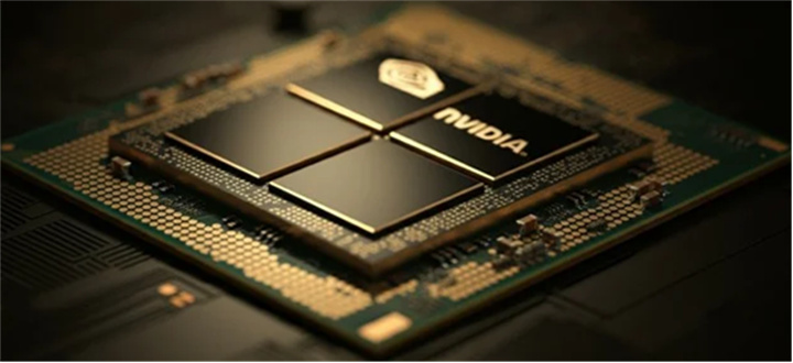
Although TSMC plans to increase the monthly CoWoS production capacity to 90000 to 110000 pieces by 2026, market demand still far exceeds supply capacity, and orders from giants such as Amazon and Microsoft have been delayed for several years. This' sweet annoyance 'is accelerating the birth of the next generation of packaging technology.
Revolutionary Breakthrough: CoPoS Technology Panel Transformation Introduction
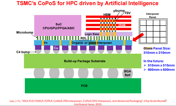
In TSMC's technology blueprint, CoPoS (Chip on Panel on Subsystem) is seen as the successor to CoWoS. This technology transforms circular wafers into square panels and replaces traditional silicon interlayers with rectangular substrates, achieving a packaging revolution of "replacing circles with squares".
The core innovation lies in:
1. Substrate form: Adopting square panels ranging from 310 × 310mm to 750 × 620mm, with an area utilization rate of over 95%.
2. Material Innovation: Replacing silicon with glass/sapphire interlayer to enhance thermal stability and cost-effectiveness.
3. Process optimization: Supports larger photomasks and single packaging of more chips.
4. Compared with similar technologies like FOPLP, CoPoS retains the intermediate layer structure and excels in signal integrity and power transmission, making it particularly suitable for high-end products that integrate GPU and HBM.
The production roadmap has been clearly defined:
In 2026, the first experimental line will be established at TSMC's Chiayi AP7 plant.
2028-2029: Achieve mass production and gradually replace CoWoS-L15.
Industry analysis suggests that CoPoS can reduce unit area costs by 20-30%, providing the possibility for the widespread adoption of AI chips. This "bigger, more cost-effective, and more efficient" technological roadmap is attracting close attention from giants such as NVIDIA.
Disruptive Idea: The Cost Revolution of CoWoP Technology
The technological advantages are obvious:
1. Cost reduction of 30-50%: Remove packaging substrates that account for 40% of the cost.
2. Shorter signal path: reduces the loss of signals from the substrate to the motherboard in traditional packaging.
3. More efficient heat dissipation: The uncovered design allows the heat sink to directly touch the chip.
However, the technological challenges are equally enormous:
1. The PCB needs to have the wiring capability of sub-10 μ m line width/spacing, far exceeding the current level of 20-35 μ m for HDI PCBs.
2. The flatness and material matching issues of large-sized PCBs.
3. Difficulty in controlling mass production yield.
According to industry sources, Nvidia is currently testing the CoWoP solution with a 450 × 450mm specification, but in the short term, its flagship Rubin chip will still use traditional ABF substrates. This reflects the numerous obstacles that new technologies face from concept to mass production.
Technical Comparison and Future Prospects
The future trend has emerged:
Short term (2-3 years): CoWoS remains mainstream, with CoWoS-L as the focus direction.
Mid term (3-5 years): CoPoS will gradually enter mass production and develop in parallel with CoWoS.
Long term (over 5 years): If CoWoP breaks through technological bottlenecks or reshapes the packaging ecosystem.
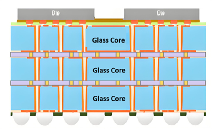
Glass substrate technology will become a key variable, and its advantages in thermal stability, signal loss, and flatness may simultaneously affect the development path of CoPoS and CoWoP.
Conclusion: Technological evolution is endless
From CoWoS to CoPoS and then to CoWoP, semiconductor packaging technology is undergoing a profound transformation from "round" to "square" and from "multi-layer" to "simplified". This transformation is not only a change in form, but also a shift in the paradigm of chip system design - expanding semiconductor integration logic from wafer level thinking to panel level dimensions.
In today's era of exponential growth in demand for AI computing power, packaging technology is no longer the "back-end link" of chip manufacturing, but the strategic frontier that determines the ceiling of computing power. Regardless of which technological route ultimately wins, the entire computing industry and end users will benefit.As an industry expert once said, "The creators of history always stand on the shoulders of their predecessors to open the next era." CoWoS laid the foundation for advanced packaging, while CoPoS and CoWoP represent a more efficient and economical future direction. In this technological evolution, we look forward to witnessing more innovative breakthroughs that are closer, more cost-effective, and more sensual.
