

Key steps in semiconductor manufacturing process:
1. Silicon chip preparation:The first step in semiconductor manufacturing is to select silicon chips as the base material. This step involves thorough cleaning and polishing of the wafer to ensure its surface is clean and flat, providing an ideal substrate for the subsequent manufacturing of electronic components.
2. Pattern making technology:Pattern making is a key step in semiconductor manufacturing, achieved through photolithography technology. Firstly, apply a layer of corrosion-resistant photoresist on the surface of the silicon chip, and then place a mask with a predetermined electronic component pattern. By irradiating with ultraviolet light, the pattern on the mask is transferred onto the photoresist, and then the photoresist in the exposed area is removed to form a precise pattern on the chip.
3. Doping process:In order to adjust the electrical characteristics of silicon chips, impurities such as boron or phosphorus are introduced. This process is called doping and is typically achieved through ion implantation techniques, where high-speed ions are injected onto the surface of the chip to form P-type or N-type semiconductors.
4. Chip deposition:Deposition of thin film material on a chip to form the layers required for electronic components. This step can be accomplished through different techniques such as chemical vapor deposition (CVD), physical vapor deposition (PVD), or atomic layer deposition (ALD) for depositing materials such as metals, oxides, and nitrides.
5. Etching process:In order to obtain the specific shape and structure of electronic components, it is necessary to remove some materials from the surface of the chip. Etching can be carried out through various techniques such as wet, dry, or plasma etching, which selectively remove materials using chemical substances or plasma.
6. Packaging steps:After completing all manufacturing steps, electronic components are packaged to become final products that can be used in electronic devices. This includes connecting components to the substrate and connecting them to other components through wires or other connection methods.
The semiconductor manufacturing process is complex, involving numerous specialized equipment and materials. The entire process, from the preparation of silicon wafers to final packaging, may take several weeks to several months. During the entire chip manufacturing process, each chip may need to go through hundreds of different process steps, so the entire manufacturing cycle may last up to 16 to 18 weeks.
Semiconductor integrated circuits are electronic components that integrate many components into a single chip to process and store various functions. Due to the fact that semiconductor integrated circuits are produced by manufacturing multiple identical circuits on a thin substrate of a wafer, the wafer is the foundation of semiconductors, just like making dough before adding ingredients when making pizza. A wafer refers to a disk made by cutting single crystal pillars of silicon (Si), gallium arsenide (GaAs), and other materials into thin slices. Most wafers are made from silicon extracted from sand. There is a large amount of silicon on Earth that can be stably supplied, and silicon has the characteristics of being non-toxic and environmentally friendly.
wafer fabrication
Firstly, the silicon dioxide (silica) in natural sand is smelted to extract industrial silicon (metallic silicon). Next, industrial silicon is purified to obtain polycrystalline silicon. Subsequently, the polycrystalline silicon was transformed into high-purity monocrystalline silicon rods using the Czochralski method. Monocrystalline silicon rods undergo processes such as grinding, cutting, chamfering, and polishing to ultimately produce silicon wafers.
After the completion of silicon wafer manufacturing, it enters the critical step of semiconductor manufacturing. Firstly, clean the silicon wafer dust-free to ensure a clean surface. Then, deposition oxidation and film coating treatment are carried out on the surface of the silicon wafer. Next, evenly apply photoresist and place the silicon wafer into the lithography machine. Using ultraviolet light to illuminate the photoresist through a photomask, achieving exposure and transferring the circuit pattern onto the silicon wafer.
After exposure, the silicon wafer enters the etching machine and uses plasma physical shock and ion implantation techniques to etch away the oxide film and silicon wafer that are not covered by photoresist, forming fins in fin field-effect transistors. After etching, clean to remove photoresist and impurities.
Subsequently, the silicon wafer enters the ion implantation machine and is injected with a high-speed and high-energy ion beam to change the carrier concentration and conductivity type of the silicon wafer, forming a PN junction. Afterwards, a protective film is applied using vapor deposition technology.
Finally, the silicon wafer is polished and polished using chemical mechanical polishing (CMP) technology to achieve a smooth surface for subsequent thin film deposition. This series of processes needs to be repeated dozens of times to complete the characterization of transistors and circuit patterns on the wafer.
After hundreds of such cycles, approximately 700 chips can be produced on a 12 inch wafer.
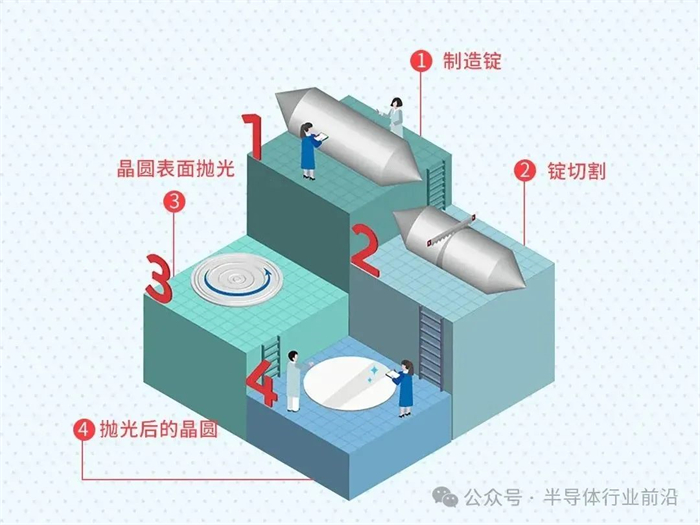
Phase 1: Manufacturing Ingot
Phase 2: Wafer Slicing
In order to turn the circular gyro shaped mirror into a disc-shaped wafer, it is necessary to use a diamond saw to cut it into thin slices of uniform thickness. The diameter of the thin film determines the size of the wafer, which can be 150mm (6 inches), 200mm (8 inches), 300mm (12 inches), and so on. The thinner the wafer, the lower the manufacturing cost, and the larger the diameter, the more semiconductor chips can be produced at once. Therefore, the thickness and size of the circle gradually become thinner and larger.
Phase 3: Lapping&Polishing of Wafer Surface
The cut wafer needs to be processed to make it smooth like a mirror. This is because the surface of the freshly cut wafer has defects and roughness, which may affect the precision of the circuit. Therefore, it is necessary to use polishing solution and polishing equipment to grind the wafer surface smooth. The wafer before processing is like being in an undressing state, so it is called a bare wafer. After multiple stages of physical and chemical processing, ICs can be formed on the surface. After the processing stage, it will become the following shape.

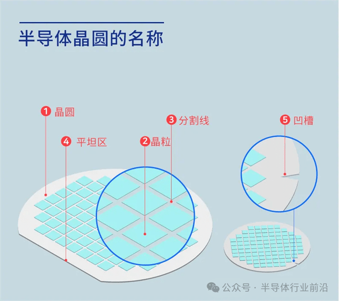
Semiconductor wafer name
1. Wafer:A wafer is the core material of semiconductor integrated circuits and is a circular board.
2. Die:Many quadrilaterals are clustered on a circular wafer. These quadrilaterals are all IC chips for integrated electronic circuits.
3. Scribe Line:It appears that the grains are stuck together, but in reality, there are certain gaps between the grains. This spacing is called the dividing line. The purpose of setting dividing lines between grains is to cut these grains one by one after the wafer processing is completed, and then assemble them into chips, as well as to leave space for diamond sawing.
4. Flat Zone:A flat zone is an area created to distinguish the structure of a wafer and is a standard line for wafer processing. Due to the extremely fine crystal structure of the wafer and its inability to be judged with the naked eye, this flat area is used as the standard to determine the vertical and horizontal orientation of the wafer.
5. Notch:Nowadays, wafers with grooves have also appeared. Compared to flat area wafers, groove wafers can produce more grains, resulting in high efficiency. The semiconductor industry includes the wafer industry that produces wafers, as well as the wafer processing industry that designs and manufactures wafers using wafers as materials - the fabrication industry (FAB). In addition, there is the assembly industry, which cuts processed wafers into grains and packages them to prevent moisture or pressure.
Aisdak always adheres to customer needs as the core, driven by intelligent equipment and precision technology, industrial software connects data flow, data+AI algorithm empowers smart warehousing in the electronics and semiconductor industries, focuses on product quality, and serves with dedication. Aisdak helps enterprises solve practical problems encountered in the scientific, standardized, digital, automated, and intelligent upgrading of intelligent warehousing, and provides customized services for intelligent warehousing equipment. In the future, AstraZeneca will continue to leverage its advantages in technical talent and resources to contribute to the transformation and upgrading of the manufacturing industry. In this process, AstraZeneca will assist more HBM manufacturing enterprises, work together to promote China's manufacturing industry to the top of the global value chain.
Part of the text and images are quoted from the forefront of the semiconductor industry