

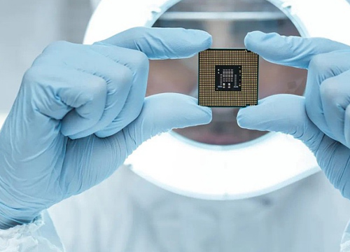
The current rapid development of AI has put forward higher requirements for data processing, and advanced packaging processes are increasingly regarded as a way to achieve higher performance of chips, which is crucial in surpassing the Moore era, and advanced packaging in the United States shows that it has become a new battlefield for technological competition.
Small chips and hybrid bonding open new frontiers
Advanced packaging has become the key to semiconductor innovation, enhanced functionality, performance and cost effectiveness. Large companies such as TSMC, Intel, and Samsung are adopting small chip and heterogeneous integration strategies, leveraging advanced packaging technologies as well as front-end scaling efforts.
The Chiplet method divides the SoC chip into multiple chips, scales only the chips with advanced technology nodes, and integrates them using 2.5D or 3D packages. This increases production and reduces costs.
Hybrid bonding (HB) is another important trend, enabling metal-metal and oxide-oxide stacking face to face with convex spacing of less than 10 µm. It is used for wafer-to-wafer hybrid bonding for applications such as CIS and 3D NAND stacking, as well as logical memory stacking for PCS, HPCS and data centers, and the ongoing development of 3D SOCs in 3D ics.
Advanced packaging requires different equipment, materials and processes than traditional packaging, such as new substrate materials, lithography processes, laser drilling, CMP and KGD testing. Advanced packaging participants have made significant investments to develop and introduce these advancements. Heterogeneous integration with advanced packaging drives semiconductor innovation and improves overall system performance while reducing costs.
Head player "shopping" advanced package
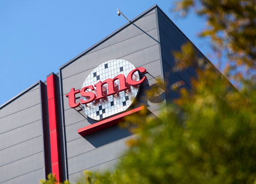
In this race for advanced packaging technology, TSMC takes the lead.
From the perspective of technology, TSMC focuses on the development of fan-out package InFO (Integrated Fan Out package) and 2.5D package CoWoS (Chip-on-Wafer-on-Substrate). SoIC (System-on-integrate-Chips) and 3D packaging。
Similar to TSMC, Intel has also laid out in the field of advanced packaging for many years, and has successively launched EMIB, Foveros and Co-EMIB and other advanced packaging technologies, but the mass production time of related products lags behind TSMC.
Due to the leading advantage of TSMC's CoWoS technology, Samsung has missed the chip foundry orders of giants such as Nvidia and Apple in China in recent years, and the market share gap with TSMC has been widening. In order to reverse the backward situation of the company's packaging technology, Samsung continued to make efforts and successively launched the I-Cube, H-Cube and X-Cube three advanced packaging technologies.
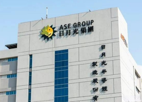
As the world's largest packaging and testing manufacturer, ASE launched the VIPack advanced packaging platform in 2022 to provide vertically connected integrated packaging solutions. The platform leverages advanced rewiring layer (RDL) processes, embedded integration, and 2.5D/3D packaging technology to achieve a three-dimensional heterogeneous package structure with ultra-high density and performance design.
For example, the world's third, the Chinese mainland's first sealed test factory Changchang Technology, has developed 2.5D/3D packaging, wafer-level packaging (WLP), stacked packaging (PoP) and other advanced packaging technology, the coverage can catch up with weekday moonlight.
The emergence of advanced packaging, let the industry see through packaging technology to promote chip high-density integration, performance improvement, miniaturization and cost reduction of the great potential, at present, artificial intelligence (AI), high-performance computing, data centers, autonomous vehicles, 5G have advanced packaging figure, the application field is gradually expanding, Major manufacturers are actively preparing for the wave of AI, and an advanced packaging technology competition has opened.
Description: The material of this article comes from the semiconductor industry and the network public information