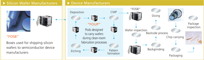
Why is there 25 wafers in a box?
In the precision world of modern technology, wafers, also known as silicon wafers, are the core components of the semiconductor industry. It is the foundation for manufacturing various electronic components such as microprocessors, memory, sensors, etc. Each wafer carries the potential of countless electronic components. So, why do we often see a box of 25 wafers? There are actually scientific considerations and the economic viability of industrial production behind this.
Revealing the reason for a box of 25 wafers:
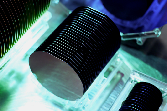
Firstly, understand the size of the wafer. The standard wafer sizes are usually 12 inches (300 millimeters) and 15 inches (300 millimeters) to accommodate different production equipment and processes. 12 inch wafers are currently the most common type because they can accommodate more chips and have a relatively balanced manufacturing cost and efficiency.
The number '25 pieces' is not accidental. It is based on the wafer cutting method and packaging efficiency. After production, each wafer needs to be cut to form multiple independent chips. Generally speaking, a 12 inch wafer can cut hundreds or even thousands of chips. However, for ease of management and transportation, these chips are usually packaged in a certain quantity, with 25 pieces being a common choice as it is neither too bulky nor ensures sufficient stability during transportation.
In addition, the quantity of 25 pieces is also beneficial for the automation and optimization of the production line. Batch production can reduce the processing cost of individual pieces and improve production efficiency. At the same time, for storage and transportation, the 25 wafer box is easy to operate, reducing the risk of damage.
It is worth noting that with the advancement of technology, some high-end products may adopt larger quantities of packaging, such as 100 or 200 pieces, to further improve production efficiency. However, for most consumer and mid-range products, a 25 wafer box is still a common standard configuration.
In summary, a box of wafers typically contains 25 pieces, which is a balance point found by the semiconductor industry between production efficiency, cost control, and logistics convenience. With the continuous development of technology, this number may be adjusted, but the basic logic behind it - optimizing production processes and improving economic efficiency - remains unchanged.
Science Popularization of Wafer Box Knowledge

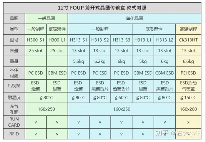
12 inch wafer fabs use FOUP and FOSB, while those under 8 inches (including 8 inches) use Cassette, SMIF POD, wafer boat boxes, etc. This means that the 12 inch wafer carrier is collectively referred to as FOUP, and the 8-inch carrier is collectively referred to as Cassette. Normally, an empty FOUP weighs about 4.2 kilograms, while a FOUP filled with 25 pieces weighs around 7.3 kilograms.
According to the research team of QYResearch (Hengzhou Bozhi), the global wafer box market sales reached 4.8 billion yuan in 2022, and are expected to reach 7.7 billion yuan in 2029, with a compound annual growth rate (CAGR) of 7.9%. In terms of product types, semiconductor FOUPs occupy the largest market share, approximately 73%. In terms of product applications, the largest application is 12 inch wafers, followed by 8-inch wafers.
In fact, there are many types of wafer carriers, such as FOUP used for transporting wafers in wafer manufacturing factories; FOSB is used for transportation between silicon wafer production and wafer manufacturing factories; CASSETTE vehicles can be used for inter process transportation and in conjunction with processes.
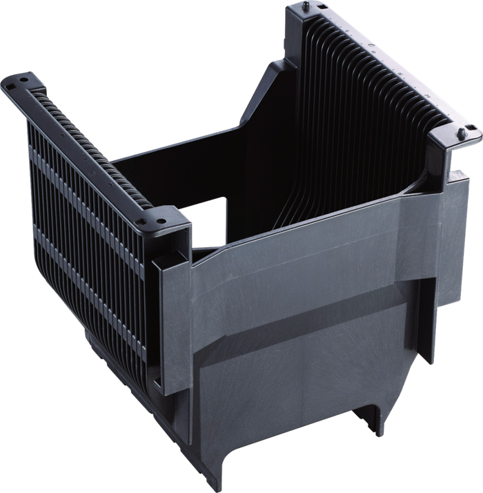
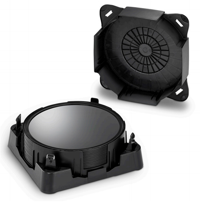
OPEN CASSETTE
OPEN CASSETTE is mainly used in processes such as transportation and cleaning within wafer manufacturing. Like FOSB, FOUP, and other carriers, it generally uses materials that are temperature resistant, have excellent mechanical properties, dimensional stability, and are durable, anti-static, low gas release, low precipitation, and recyclable. Different wafer sizes, process nodes, and materials used in the process vary. Generally, materials include PFA, PTFE, PP, PEEK, PES, PC, PBT, PEI, COP, etc. The product is designed with a capacity of 25 pieces.
OPEN CASSETTE can be used in conjunction with corresponding Wafer Cassette Box products for wafer storage and transportation between processes, reducing wafer contamination.
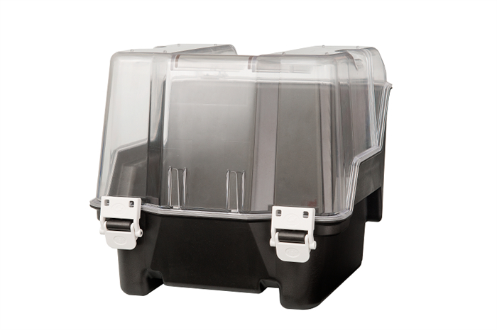
OPEN CASSETTE can be used in conjunction with customized Wafer Pod (OHT) products for automated transfer, automated access, and more sealed storage between processes in wafer and chip manufacturing.
Of course, OPEN CASSETTE can be directly made into CASSETTE products, and the structure of the product Wafer Shipping Boxes is like this, as shown in the following figure. Can meet the transportation needs of wafers from wafer manufacturing plants to chip manufacturing plants. CASSETTE and its derived products can basically meet the requirements of transportation, storage, and inter factory transportation between various processes in wafer fabs and chip factories.
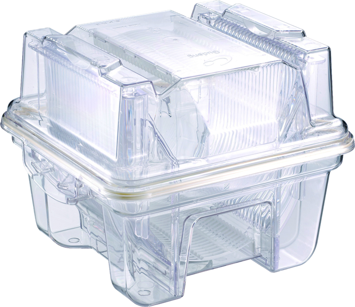
Front opening wafer transport box FOSB
Front Opening Shipping Box (FOSB) is mainly used for transporting 12 inch wafers between wafer manufacturing plants and chip manufacturing plants. Due to the large size of wafers and higher requirements for cleanliness; By using special positioning plates and shock-absorbing designs, impurities generated by wafer displacement friction are reduced; The raw materials are made of low release gas materials, which can reduce the risk of gas pollution to the wafer. Compared to other transport wafer boxes, FOSB has better airtightness. In addition, FOSB can also be used for storing and transferring wafers between various processes in the packaging line factory.
FOSB is usually made into a pack of 25 pieces, which can be manually operated in addition to automatic access through the Automated Material Handling System (AMHS).
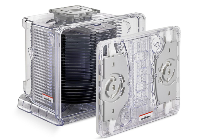
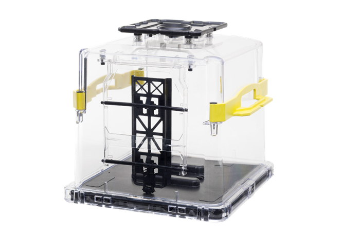
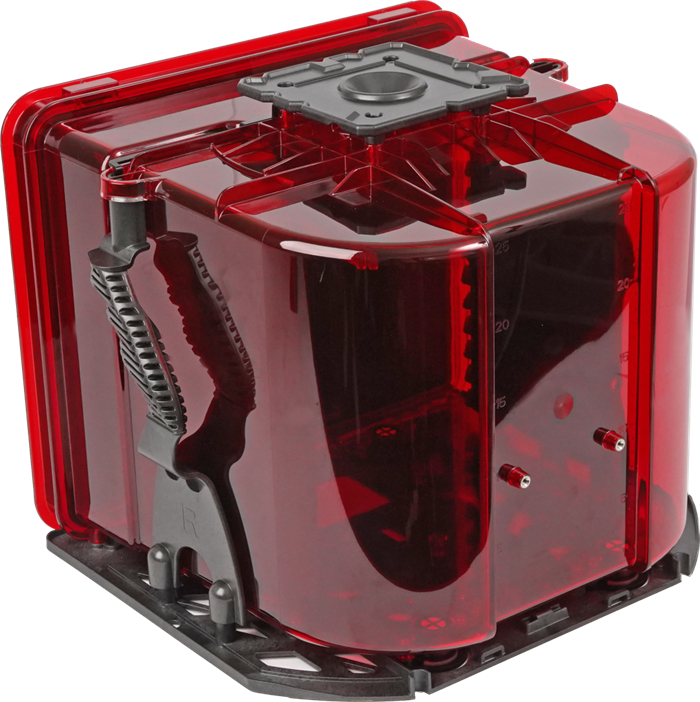
Front opening wafer transfer box FOUP
Front Opening Unified Pod (FOUP) is mainly used for the protection, transportation, and storage of wafers in Fab factories. It is an important transfer container for automated transfer systems in 12 inch wafer factories. Its most important function is to ensure that every 25 wafers are protected from being contaminated by external dust during transportation between each production machine, thereby affecting yield. Each FOUP has various connection plates, pins, and holes for the FOUP to be located on the loading port and operated by AMHS. It adopts low gas release and low moisture absorption materials, which can significantly reduce the release of organic compounds and prevent wafer contamination; At the same time, excellent sealing and inflation function can provide a low humidity environment for the wafer. In addition, FOUP can be designed in different colors, such as red, orange, black, transparent, etc., to meet process requirements and distinguish different processes and procedures; Generally, FOUP is customized by customers based on differences in Fab factory production lines and machines.
In addition, POUP can be customized into special products for packaging manufacturers based on different processes such as TSV, FAN OUT, etc. in the chip post packaging, such as SLOT FOUP, 297mm FOUP, etc. FOUP is reusable and has a lifespan of 2-4 years. FOUP manufacturers can provide product cleaning services to ensure that contaminated products can be reused.
Contactless horizontal wafer shippers are mainly used for the transportation of finished wafers, as shown in the following figure. Entegris transport box uses support rings to ensure that wafers do not come into contact during storage and transportation, while also having good sealing properties to prevent impurity contamination, wear, collision, scratches, degassing, and other issues. The product is mainly suitable for Thin 3D, lens or inflated wafer applications, including 3D, 2.5D, MEMS, LED, and power semiconductors. The product is equipped with 26 support rings, with a wafer capacity of 25 (thickness can vary), and wafer sizes including 150mm, 200mm, and 300mm.
Part of the text and images are cited in the semiconductor industry chip sound