CoWoS packaging technology

CoWoS(Chip on Wafer on Substrate)The architecture completely subverts the traditional chip packaging method by introducing 2.5D horizontal stacking and 3D vertical stacking configurations. This innovative approach allows different processors and memory modules to be stacked layer by layer, building a highly integrated system through tight chip to chip interconnections. CoWoS technology utilizes through silicon via (TSV) and micro bump technology, which significantly shortens the interconnect length, reduces power consumption, and enhances signal integrity compared to traditional two-dimensional packaging methods.
In practical applications, CoWoS technology can seamlessly integrate advanced processing units such as GPUs and artificial intelligence accelerators with high bandwidth memory (HBM) modules. This integration is particularly critical for artificial intelligence applications, as these applications have extremely high requirements for large-scale computing power and fast data access. By tightly configuring processing and memory components, CoWoS technology minimizes latency, improves data throughput, and brings unprecedented performance improvements to memory intensive tasks. This integration approach greatly optimizes the performance of artificial intelligence and other high-performance computing applications, resulting in significant improvements in processing speed and efficiency.
The advantages of CoWoS packaging
CoWoS (Chip on Wafer on Substrate) packaging technology has several significant advantages, which make it extremely important in high-performance computing and advanced semiconductor manufacturing fields:
High density integration: CoWoS technology allows for the integration of multiple chips, including processors, memory, and other functional modules, in a single package, achieving high-density system integration. This integration method can significantly reduce the physical distance between chips and improve the overall system performance.
Shortening Interconnection Length: By using through silicon via (TSV) technology, CoWoS can achieve vertical interconnection between chips, significantly reducing signal transmission paths, signal delay, and power consumption.
Enhanced signal integrity: Due to the shortened interconnect length, signal attenuation and interference during transmission are reduced, thereby improving signal integrity and reliability.
Reduce power consumption: Shorter interconnect paths and optimized power distribution networks can help reduce overall power consumption, which is particularly important for applications such as mobile devices and data centers that have strict energy efficiency requirements.
Improve bandwidth and throughput: CoWoS technology supports the integration of high bandwidth memory (HBM), which provides much higher bandwidth than traditional DDR memory and is ideal for applications that require large amounts of data processing, such as artificial intelligence and graphics processing.
Reducing packaging size: Through 3D stacking technology, CoWoS can achieve more functionality and higher performance in a smaller packaging size, helping to reduce the size of electronic devices.
Improving thermal management efficiency: CoWoS packaging allows for more efficient distribution and heat dissipation, helping to maintain stable temperatures in high-performance computing and avoid performance degradation or damage caused by overheating.
Support heterogeneous integration: CoWoS technology can integrate chips from different process nodes to achieve heterogeneous integration, which is very useful for integrating chips from advanced and mature processes, and can optimize cost and performance.
In summary, CoWoS packaging technology provides powerful technical support for high-performance computing and advanced semiconductor applications through its high integration, optimized interconnects, and efficient energy utilization.
Market Trends of CoWoS Technology
1. Demand driven factors
Technological development: The development of technologies such as artificial intelligence, cloud computing, big data analysis, and mobile computing has driven the demand for high-performance computing devices.
The improvement of computing power: The high demand for computing power in modern society has promoted the development of artificial intelligence chips.
Market growth: TrendForce data shows that the shipment volume of artificial intelligence servers has significantly increased and is expected to continue to grow in the coming years.
High end chip demand: The demand for high-end chips such as GPUs using high specification HBM has increased.
2. Supply and demand dynamics
Capacity constraints: Due to increasing demand, TSMC's CoWoS packaging capacity is tight, affecting the output of artificial intelligence chips.
Capacity expansion: TSMC plans to increase CoWoS packaging capacity and invest in new factories to alleviate supply-demand imbalances.
Market competition: Other Taiwanese companies such as UMC, Sunlight Technology Holdings, and Licheng Technology are entering the CoWoS advanced packaging market to provide alternative solutions.
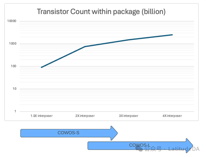
The CoWoS technology currently used is divided into three categories:
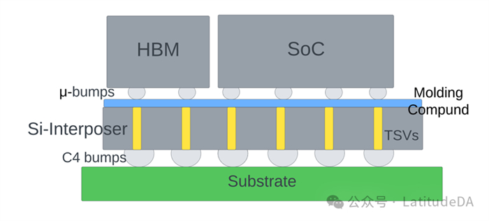
CoWoS-S: This technology uses single-chip silicon inserts and through silicon vias (TSVs) to facilitate direct transmission of high-speed electrical signals between chips and substrates. However, there is a yield issue with the on-chip silicon intercalation layer.
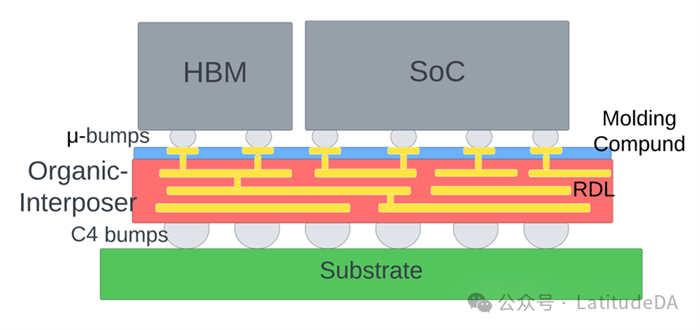
CoWoS-R: This technology replaces the silicon intercalation of CoWoS-S with organic intercalation. Organic intercalation has fine pitch RDL, which can provide high-speed connections between HBM and chips or even chips and substrates. Compared with CoWoS-S, CoWoS-R has higher reliability and yield because the organic intermediate film itself has flexibility and can serve as a stress buffer to alleviate reliability issues caused by mismatched thermal expansion coefficients between the substrate and the intermediate film.
CoWoS-L package: This package uses local silicon interconnects (LSI) and RDL add ons to form a recombination add in (RI). In addition to the RDL plugin, it also retains the attractive feature of CoWoS-S, which is through silicon via (TSV). This also alleviates the yield issue in CoWoS-S caused by the use of large silicon inserts. In some implementation schemes, it can also use through insulator via (TIV) instead of TSV to minimize insertion loss.
Understand CoWoS packaging components
CoWoS-L (Chip on Wafer on Substrate) is an advanced chip end of pipe assembly technology used to integrate multiple wafer chips (such as SoC, HBM, etc.) together. CoWoS-L technology uses an intermediate film as a key raw material, on which wafer chips are stacked to achieve effective connection and communication between chips.
The following is the specific process of CoWoS-L technology:
Intermediate film manufacturing: First, manufacture the intermediate film, which is the key raw material for CoWoS-L technology. Multiple wafer chips can be installed on the intermediate film to achieve effective connection and communication between chips.
TIV (Through Island Via) manufacturing: Manufacturing through insulated vias (TIVs) on wafer bare chips for connecting wafer chips and intermediate films.
KGD (Known Good Die) installation: Fill molding compound between TIV and wafer chip, and use CMP (Chemical Mechanical Polishing) process to obtain a flat surface. Then install known good chips (KGD) on the wafer chip.
RDL (Distribution Layer) manufacturing: Two RDL layers are manufactured, one located on the front side of the intermediate film, connecting the chip and substrate through μ bumps, and the other located on the back side of the intermediate film, connecting the intermediate film and substrate through C4 bumps.
Deep trench capacitors (DTC): CoWoS-L technology also uses deep trench capacitors (DTC), which can provide high capacitance density and improve the electrical performance of the system. These capacitors can serve as charge reservoirs to meet the instantaneous current requirements for high-speed computing applications.
Application of CoWoS Technology
Compared to older packaging technologies such as System on Chip (SiP), CoWoS technology can support more transistors in the packaging. This technology is most suitable for applications that require large amounts of parallel computing, processing of large vector data, and high memory bandwidth.
Some applications of CoWoS include:
High Performance Computing (HPC)
Artificial Intelligence (AI) and Machine Learning (ML)
Network and Data Center
Graphics Processing Units (GPUs) and Games
Aisdak always adheres to customer needs as the core, driven by intelligent equipment and precision technology, industrial software connects data flow, data+AI algorithm empowers smart warehousing in the electronics and semiconductor industries, focuses on product quality, and serves with dedication. Aisdak helps enterprises solve practical problems encountered in the scientific, standardized, digital, automated, and intelligent upgrading of intelligent warehousing, and provides customized services for intelligent warehousing equipment. In the future, AstraZeneca will continue to leverage its advantages in technical talent and resources to contribute to the transformation and upgrading of the manufacturing industry.