
IC packaging substrate plays a crucial role in modern electronic products, which directly affects the performance, power consumption, heat dissipation and other aspects of integrated circuits.
Ceramic substrate: Using ceramic as substrate material, it has excellent high-frequency characteristics and heat dissipation performance.
Metal substrate: The use of metal material as a substrate, with good heat dissipation performance.
Double-sided substrate: A substrate with two conductive layers, usually with pads or balls on both sides.
Multilayer substrate: Composed of multiple insulating and conductive layers for high-density packaging.
QFN (Quad Flat No-leads) : pin-less package, the pins are located on all sides of the package.
SIP (System in Package) : Multiple chips are packaged on the same substrate to form a package unit.
High-density interconnect substrate: Used for high-density packaging, requiring a compact pin layout and good signal integrity.
Heat dissipation substrate: Specially designed for high heat dissipation requirements of the package, with good heat dissipation performance.
Flexible substrate: The flexible substrate manufacturing process is suitable for applications that require bending or folding.
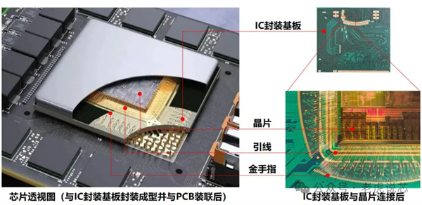
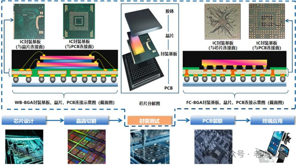
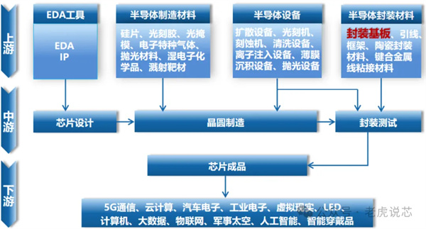
After the chip is designed and manufactured, it needs to be packaged and tested, and the IC packaging substrate is used for the IC packaging link, and then the PCB plug-in, patch and other processes.
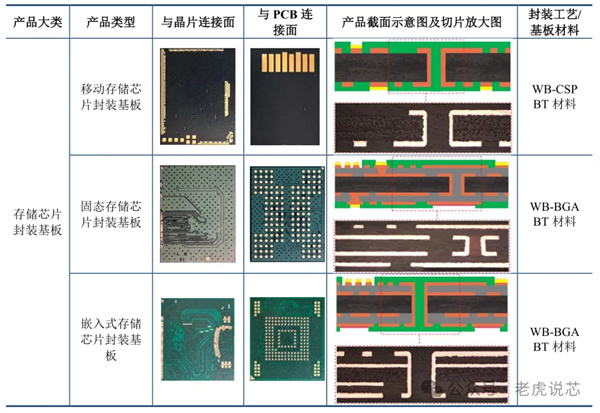
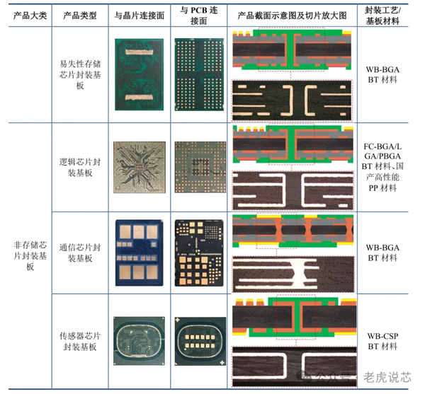
IC packaging substrate and corresponding applications are as follows: Mobile memory chip package board (corresponding to U disk), solid state memory chip package board (corresponding to solid state memory), embedded memory package board (corresponding to embedded memory), volatile memory chip package board (corresponding to dynamic memory), logic chip package board (corresponding to logic chip), communication chip package board (corresponding to SIM card, etc.), sensor chip seal Install the substrate (corresponding to fingerprint sensor, etc.).

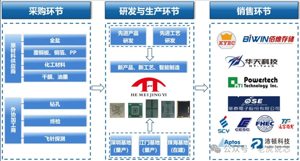
The company's downstream customers are divided into memory customers (such as Baiwei) and packaging and testing customers (such as Huatian). The main requirements of the memory class customers are focused on the packaging substrate of the memory product, while the packaging test class customers need the packaging substrate for chip packaging testing. By working with these different types of customers, packaging substrate companies can meet the needs of different areas, expand market share and enhance competitiveness.
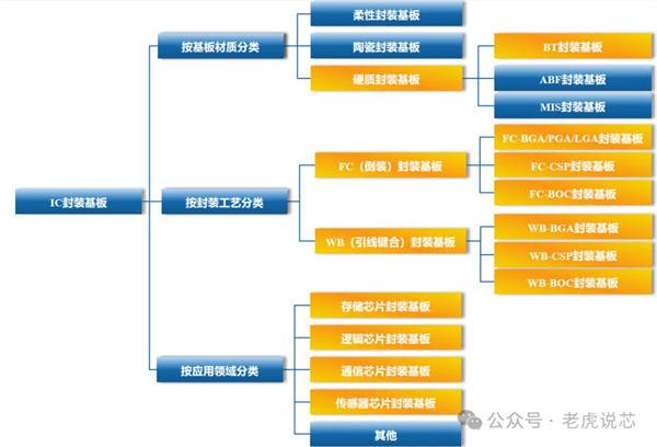
The specific categories, examples and applications of IC packaging substrates in the industry are as follows:

The other is the package substrate applied to the digital chip, the digital chip includes baseband chip, application processor chip, memory card chip, etc. These digital chips typically require highly integrated and high-performance packaging substrates. Common digital Chip packaging substrates include WBBGA (Wire Bond Ball Grid Array), WBCSP (Wire Bond Chip Scale Package), and FCBGA (Flip Chip Ball Grid) Array), FCCSP (Flip Chip Chip Scale Package), etc.

The key to the Tenting process is to use methods such as etching to remove excess copper from the surface of the copy-clad plate, thereby forming the required conductive circuit. However, due to the limitation of the etching process, the line needs to retain a certain amount of base copper during the etching process to avoid the line being corroded. Therefore, the Tenting process is often difficult to make lines with line width/line spacing less than 30/30μm.
The key to the mSAP process is to cover the unwanted wires with a dry film, and then thicken the copper on the ultra-thin copper foil of the coppered plate to form the required conductive wires. Then the unwanted lines are quickly removed by a flash etching process, and finally a complete conductive line is obtained. The mSAP process has the ability to produce products with line width/line spacing as small as 25/25μm and below.
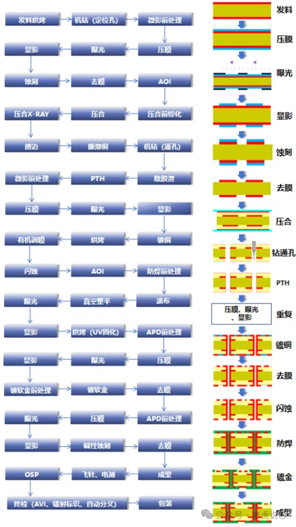
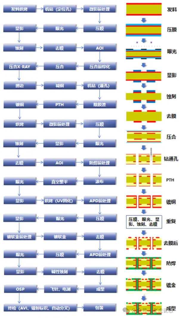
Issue baking: By removing moisture from the surface of the plate, stabilize the size of the substrate, reduce thermal stress, and ensure the stability of the subsequent process.
Pressing film: The photosensitive dry film is covered on the copper surface of the substrate to prepare for subsequent exposure and development.
Exposure: Using laser scanning technology to image directly on the substrate to form circuit patterns.
Development: The dry film of the exposed part is cured and the dry film of the unexposed part is removed by the developer treatment.
Copper plating: A layer of copper of a certain thickness is chemically plated on the surface of the copper foil to increase electrical conductivity.
Removing film: Using the film removing liquid to remove the dry film covered by the plate surface, exposing the copper foil that needs to be eroded back.
Etching: By rapid etching or ordinary etching process, the desired circuit pattern is formed.
AOI: Inspects etched lines with automated optical inspection technology to ensure quality.
Pressing: the copper foil, PP and copper clad plate are superimposed and bonded into one under high temperature and pressure to form a multi-layer plate.
Drilling: Drilling the copper-clad plate with a drill to prepare for the subsequent PTH process.
PTH: Plated through holes to form a conductive copper layer to realize the connection of double-sided copper foil.
Solderproof: Cover the solderproof paint material to protect the line from oxidation or contamination.
Gold plating: A layer of gold is plated on the gold finger or nickel surface to improve electrical conductivity and corrosion resistance.
Molding: The base plate is milled to standard dimensions by milling cutter.
OSP: Anti-oxidation treatment of brazing pad by degreasing agent.
Final inspection: Complete inspection of the finished product to ensure that the product meets the specifications.
Together, these processes make up the manufacturing process of the IC packaging substrate, and each step is critical and affects the quality and performance of the final product.
Some of the images are quoted from the "Tiger said core" public number