
1、 Definition and division criteria
(1) Advanced Process
Definition: Refers to the semiconductor manufacturing process at the forefront of current technology, usually marked by the minimum line width of the transistor gate (such as nanometer/nm).
Typical range:
7nm and below (such as TSMC 3nm, Samsung 2nm, Intel 18A).
In some scenarios, 14/16nm~7nm is also considered a "quasi advanced process".
Core features:
Use three-dimensional structures such as FinFET (FinFET) or GAA (Ring Gate Transistor).
The popularization of extreme ultraviolet lithography (EUV) technology.
High transistor density (billions of transistors per square millimeter).
(2) Mature Process
Definition: A standardized technology, stable production, and low-cost process, typically referring to processes of 28nm and above.
Typical range:
28nm~180nm (such as 40nm, 65nm, 90nm, etc.).
Some special applications, such as power semiconductors, still use micrometer level (μ m) processes.
Core features:
The planar FET structure is the main structure.
Deep ultraviolet lithography (DUV) technology can meet the requirements.
Low research and development costs, high yield (usually>95%).
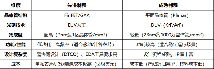
2、 Comparison of Technical Differences
3、 Application scenarios
Advanced manufacturing process
High performance computing: CPU (such as Apple A-series), GPU (NVIDIA), AI chips (such as TPU).
5G/6G communication: baseband chip (Qualcomm Snapdragon), RF front-end.
Frontier fields: autonomous driving chips (Tesla FSD), quantum computing interface chips.
Mature process
Internet of Things (IoT): sensors, MCUs (such as STM32).
Automotive electronics: ECU, power management chip (PMIC).
Industrial and home appliances: motor control, display driver chips.
Analog chips: RF, power devices (such as IGBT).
(Note: Mature processes account for over 70% of global semiconductor production capacity, particularly in the automotive and industrial sectors where demand continues to grow.)
4、 Advanced Manufacturing Global Competitive Player Introduction
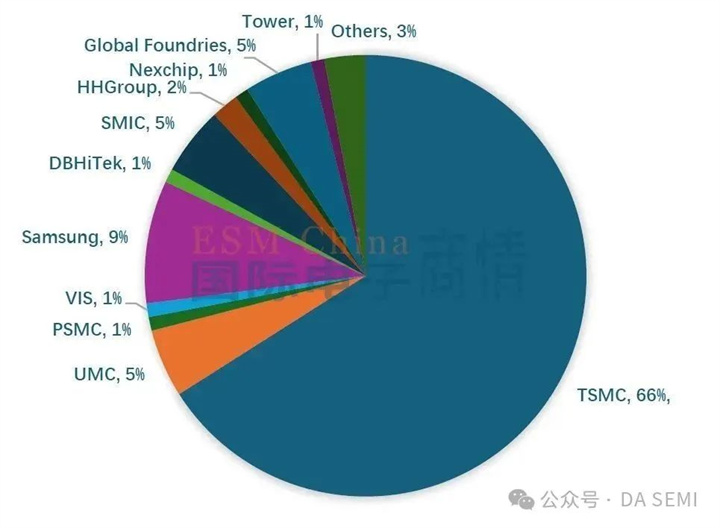
By 2025, the proportion of global wafer foundry revenue will be accounted for, with 90% of global wafer foundry revenue being held by the five major wafer foundries.
At present, the main players competing in the field of advanced processes worldwide include TSMC, Samsung, and Intel.
TSMC accounts for about 66%, Samsung accounts for about 9%, and UMC, SMIC, and Global Foundries each account for 5%.
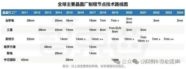
TSMC has announced the successful mass production of 3nm fin field-effect transistor process technology and is advancing the research and development of 2nm and 1nm technologies. Samsung is also actively developing its advanced process technology, with the goal of mass producing 3nm chips set many years ago.
5、 Evolution of Advanced Process Technology and Analysis of Industrial Impact
1. Challenges and Development of Multi Chip Interconnection and Hypernode Architecture in AI Computing
In recent years, the core focus of the semiconductor industry has mainly been on the improvement of single-chip computing power. However, with the rapid development of AI large-scale models (such as multi billion level parameter models), the computing paradigm is gradually evolving towards multi chip interconnect communication intensive architectures. This trend places higher demands on low latency interconnect technologies such as chiplets and 3D packaging, as well as cross node parallel computing capabilities.
Specific challenges include:
Tensor parallelism and expert model distribution require high bandwidth and low latency interconnection;
The rise of Super Node architecture, which optimizes distributed training efficiency by increasing the density of computing and storage resources within a single node;
Optimizing energy efficiency ratio becomes key, and the computational efficiency under AI load needs to be improved by combining process miniaturization and architecture innovation.
2. Huawei drives the coordinated development of the domestic semiconductor industry chain
Huawei's breakthrough in the field of advanced processes has significantly accelerated the localization process of the domestic semiconductor industry chain, manifested in:
Mature process demand rebounds: In Q2 2024, orders for analog chips (PMIC, signal chain, etc.) exceeded expectations, mainly driven by inventory replenishment for industrial and automotive customers. The capacity utilization rate of 8/12 inch wafer fabs is close to full load, and the growth trend is expected to continue until the end of the year.
Accelerated research and development of advanced processes: Domestic leading OEM companies (such as SMIC) continue to increase their R&D investment, and it is expected that from 2024H2 onwards, they will enter a critical stage of expansion and technological iteration, and their long-term competitiveness is expected to further improve.
3. Challenges and structural opportunities in the domestic semiconductor industry chain
Affected by US export controls, domestic high-performance computing chip design companies (such as AI accelerators and server CPU manufacturers) are facing transistor scale limitations, driving a surge in demand for local advanced process capacity.
The core trends include:
The scarcity of advanced processes is highlighted: although multiple domestic manufacturers have laid out nodes of 14nm and below, technology leaders (such as SMIC N+1/N+2 processes) still have a generation gap advantage of more than 2 years.
Accelerate the localization of equipment chain: Key equipment links such as photolithography, etching, and thin film deposition have become investment priorities, and the penetration rate of local supply chains continues to increase.
4. Prospects for the semiconductor equipment industry and recommendations for core targets
In 2024, the domestic semiconductor equipment industry will undergo a phase of adjustment, and the current valuation is attractive.
Future driving factors include:
Storage technology iteration: DRAM/NAND will enter a new process cycle in 2025, driving device demand to rebound.
Policy support for mature process expansion: With the goal of increasing global market share, local equipment manufacturers (such as Northern Huachuang and Zhongwei Company) will benefit first.
5. Multi link collaborative breakthroughs in the domestic computing power industry chain
The domestic AI computing ecosystem covers design, manufacturing, packaging, and supporting hardware, with core components including:
PCB/Packaging Substrate: Shennan Circuit and Xingsen Technology are leading in the field of high-density interconnect (HDI) technology.
Chip design: Cambricon and Yuntian Lifei enhance cost-effectiveness through differentiated architectures such as NPU+integrated storage and computing.
Server integration: The increase in localization rate drives the growth of the market share of complete machine manufacturers.
6. The catalytic effect of Huawei's 384 core supernode on the domestic computing power sector
Despite the short-term constraints of increasing production capacity, the launch of Huawei Atlas 900 super node cluster marks a new stage for domestic computing architecture.
The core beneficiaries include advanced manufacturing (SMIC (expanding 14nm FinFET production)) and advanced packaging (HBMlike customized storage).
7. The core position of storage chips in computing infrastructure
Storage bandwidth has become the key to breaking through the bottleneck of computing power, and industry trends include: increasing penetration rate of DDR5/LPDDR5; Integrated storage and computing technology: alleviates the "memory wall" problem through 3D stacking (such as HBM).
6、 Summary
Advanced manufacturing processes are the high ground of technological competition, but they rely on huge investments and cutting-edge equipment.
Mature processes are the cornerstone of the semiconductor industry, supporting the vast majority of practical applications.
In the future, the two will coexist for a long time, with advanced processes evolving towards 3D integration (Chiplets), and mature processes revitalizing through characteristic processes such as BCD and SiC.