1. Thickness of silicon wafer
In the front-end process of semiconductor manufacturing, wafers need to have sufficient thickness to meet the requirements of mechanical strength and warpage, in order to be processed and transported within and between equipment.
150mm (6-inch) wafer
Standard thickness: approximately 675 microns
Range: typically between 650 microns and 700 microns
200mm (8-inch) wafer
Standard thickness: approximately 725 microns
Range: typically between 700 microns and 750 microns
300mm (12 inch) wafer
Standard thickness: approximately 775 microns
Range: typically between 750 microns and 800 microns
2. Advantages of wafer thinning
1. Improve heat dissipation performance
The thinned wafer can dissipate heat more efficiently, thereby reducing the temperature during device operation.
Thermal management is crucial in high-power devices such as power semiconductors, RF devices, etc. Thinning wafers can increase the ratio of surface area to volume, accelerate heat conduction and diffusion, and avoid device failure caused by overheating.
2. Improve mechanical performance
The flexibility enhancement of thin wafers is helpful for subsequent operations in packaging processes. For example, in flip chip packaging, the thinned wafer is easier to adhere to the substrate.
For certain special application scenarios, such as flexible electronic devices, thin wafers can better adapt to the needs of bending or deformation.
3. Reduce parasitic capacitance
After thinning the wafer, the volume of silicon material is reduced, thereby reducing parasitic capacitance.
Parasitic capacitance can affect the signal transmission speed and power consumption of circuits, especially in high-frequency circuits and high-speed digital circuits. Reducing parasitic capacitance can improve overall performance.
4. Reduce device power consumption
Reducing the thickness of the wafer can directly reduce the resistance loss and charge storage requirements inside the device, thereby reducing power consumption.
Especially in mobile devices and portable electronic products, reducing power consumption can extend battery life.
5. Optimize packaging size
Thin wafers can significantly reduce the final packaging volume, meeting the demand for miniaturization and lightweighting in modern electronic devices.
For example, in consumer electronics fields such as smartphones and tablets, thinning wafers can help achieve more compact designs.
6. Enhance performance consistency
In multi-layer stacked 3D integrated circuits (3D ICs), thinning the wafer can ensure higher alignment accuracy between different layers, thereby improving device consistency and reliability.
7. Reduce manufacturing costs
Although thinning wafers requires additional process steps, it can indirectly reduce costs by improving yield and reducing material waste.
Meanwhile, the application of thin wafers can reduce the usage of packaging materials and further optimize production efficiency.
3. Wafer thinning process
The wafer thinning process generally uses methods such as mechanical grinding and chemical mechanical polishing (CMP) to achieve wafer thinning. The specific process includes preliminary preparation, thinning operations (such as rough grinding, fine grinding, and polishing), and post-processing (such as cleaning residues, measuring flatness, and quality inspection). In advanced packaging technologies such as 2.5D and 3D packaging, the required chip thickness may be as low as 30 microns.
4. Wafer thinning technology
1. Mechanical grinding
Mechanical grinding is a traditional thinning method that involves cutting the surface of a wafer using a high-speed rotating grinding wheel. The characteristic of this method is high efficiency and low cost, but it may lead to surface damage and warping of the wafer. Mechanical grinding is usually divided into the following steps:
Rough grinding: Remove excess material from the surface of the wafer.
Fine grinding: further reducing thickness and improving flatness.
2. Chemical mechanical polishing (CMP)
Chemical mechanical polishing combines chemical reactions and mechanical actions to achieve a more uniform thinning effect. CMP technology is widely used in ultra precision machining, which can maintain wafer flatness while thinning. The main steps of CMP include:
Chemical etching: using chemical reagents to soften the surface of the wafer.
Mechanical polishing: removing materials through polishing pads and polishing solution.
3. Laser thinning
Laser thinning is an emerging technology that uses high-energy laser beams to directly remove materials from the surface of wafers. This method has the characteristic of non-contact, which can avoid the influence of mechanical stress on the wafer, but the equipment cost is relatively high.
4. Ion implantation thinning
Ion implantation thinning achieves the effect of thinning by accelerating charged particles to bombard the surface of the wafer, causing physical and chemical changes. This method is suitable for the thinning requirements of specific materials, but requires complex equipment support.
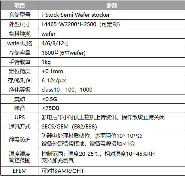
i-Stock Semi-wafer stocker
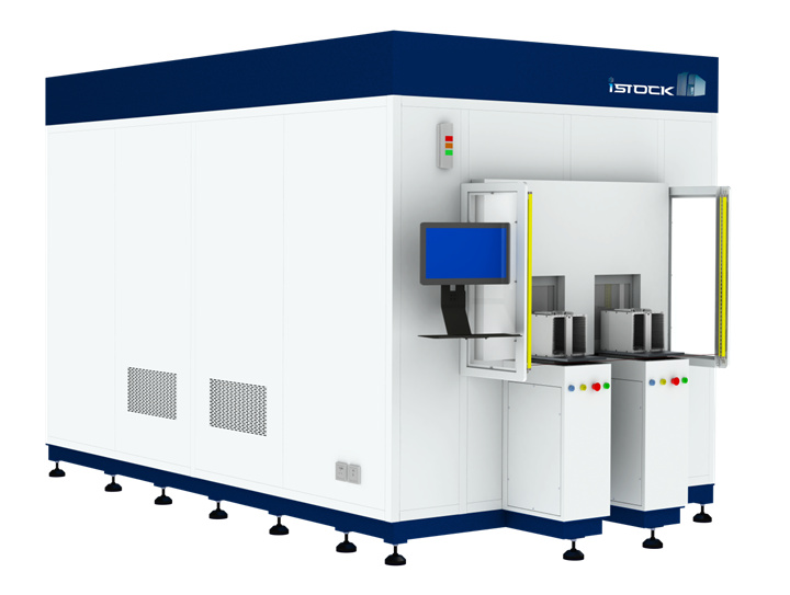
Product Introduction
I-Stock Semi wafer stocker is a new, efficient, safe, and stable wafer storage device in China's advanced semiconductor wafer intelligent storage applications. Its equipment implements unmanned, precise, and intelligent management of semiconductor wafers with "one item, one code, one storage location", and seamlessly integrates with ERP, MES, WMS and other systems to achieve intelligent wafer storage, thereby improving efficiency, reducing labor, and minimizing the risk of material errors and manual waste disposal. At present, this device has been widely used in semiconductor intelligent warehousing applications.
Product parameters